Terahertz (THz) imaging systems are currently one of the most attractive topics in optoelectronics. As all systems active elements are getting smaller, passive optical components as well required to be more compact. In this case optical properties and compactness of graphene makes it suitable for this application. To make a functional diffractive element, graphene requires to absorb THz radiation. Since it is almost completely transparent in this frequency range, graphene's transmittance can be controlled by using chemical, electrical or optical doping [1].
In this work optical modulation is chosen as contactless method.
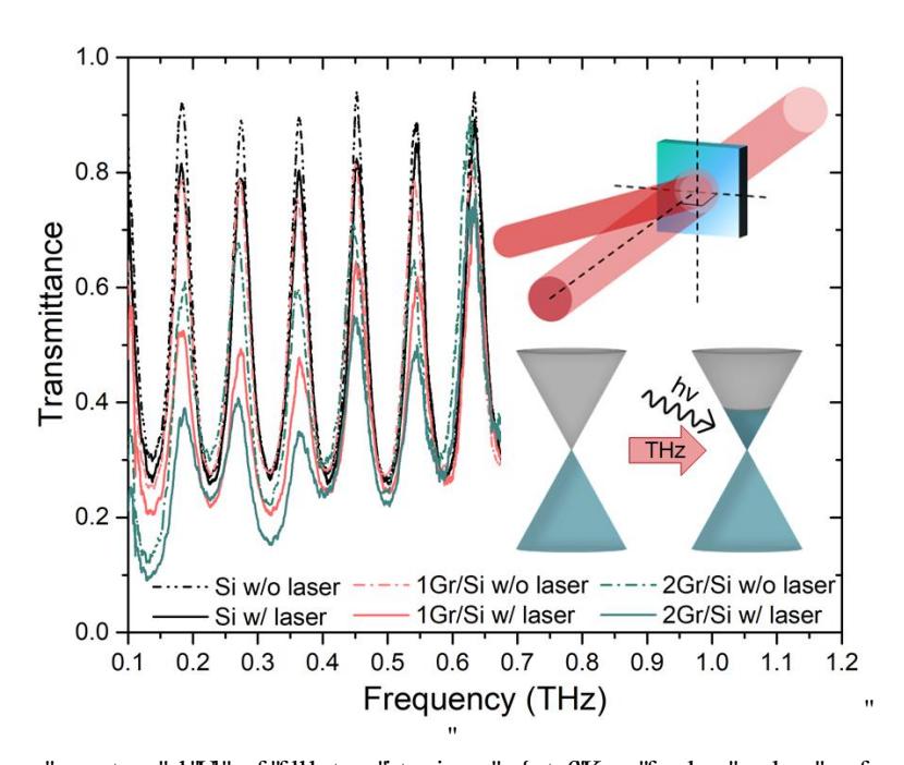
Three types of samples were fabricated in order to investigate optical modulation of mono and bi-layer graphene. As graphene is not a free-standing material, it was transferred on silicon (Si) substrate, which is transparent in THz range. Therefore, the first sample is a single graphene layer on Si. The second sample is two graphene layers on Si which were transferred one by one. The third sample is pure Si wafer which served as a reference to the first two samples.
Optical modulation was achieved by using pumping laser to generate free carriers in Si substrate. Carriers are transferred to graphene layer and due to its higher carrier mobility, graphene's transmittance of THz radiation is reduced [2].
In order to evaluate modulation depth of all three samples, transmittance spectra were measured using THz frequency-domain spectrometer. Spectra are depicted in Fig. 1. Results showed that due to photoexcitation, the modulation depth of bi-layer graphene goes up to 42%.
Photo-modulation features of graphene-on-silicon prepared using different technological approaches will be discussed in details.