The AlGaN/GaN high electron mobility transistors (HEMTs) used in high power and high frequency applications usually are grown on silicon carbide (SiC) substrate. The common approach to compensate for the lattice mismatch and to reduce the dislocation density in these structures is to grow thick GaN buffer doped with deep acceptors such as Fe or C which compensate residual doping of an n-type GaN on top of the AlN nucleation layer (NL). However, this approach reduces the advantage of SiC high thermal conductivity. Also, the acceptor-type impurities in a thick GaN buffer introduce the deep charge trapping centers resulting in the increase of low-frequency noise [1]. To solve this, a new heteroepitaxy approach has been developed recently, which is based on the hot-wall metalorganic vapor deposition (MOCVD) and allows to grow high structural quality AlGaN/GaN HEMT structures without thick GaN buffer [2]. It could be expected that this technology will reduce effects of traps from GaN:C buffer, but thick acceptor doped GaN buffer is important for reduction of threading dislocations density.
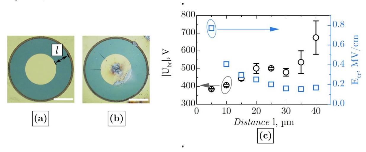
In this work, the “buffer-free” AlGaN/GaN heterostructure was used to develop Schottky barrier diodes (SBDs) and HEMTs studying the performance of realistic devices under high DC voltages and in radio frequency (RF) regimes. The voltage-current, the noise, and the gain characteristics demonstrated the improved thermal stability of “buffer-free” AlGaN/GaN heterostructure in comparison to a standard AlGaN/GaN heterostructures but with thick GaN buffer [1,3]. The SBDs demonstrated the breakdown fields up to 0.8 MV/cm. Hall measurements revealed thermally stable two-dimensional electron gas (2DEG) density N2DEG = 1013 cm-2 in the range from room temperature (300 K) down to liquid nitrogen (77 K) with the respective mobility values of μ = 1.7·103 cm2/V·s and μ = 1.0·104 cm2/V·s. Meanwhile the HEMTs demonstrated a maximum drain current and the transconductance values to be as high as 0.5 A/mm and 150 mS/mm, respectively for the transistors with the gate length LG = 5 μm. Low-frequency noise characterization of HEMTs revealed the effective trap density values to be below 1019 cm-3eV-1. The analysis of transistors RF characteristics revealed fT and fmax values to be up to 1.3 GHz and 6.7 GHz, respectively, demonstrating the figure of merit FOM=fT×LG to be up to 6.7 GHz μm.