The last decade huge interest in devices, operating in telecommunication wavelengths window (from 1 µm to 1.5 µm) was observed. Traditionally the active area of such components is fabricated using heterostructures of A3-B5 semiconductor compounds, such as InGaAsP or InGaAlAs. These devises are sensitive to temperature, and stabilization of parameters require external coolers [1]. To obviate disadvantages and fulfill the main requirements for semiconductors technologies - high efficiency and low costs, the performances of components must be improved. This could be achieved replacing usual heterostructures by new more attractive material.
GaAsBi, namely bismide alloy, exhibit unique physical properties, including a large energy bowing effect, less temperature sensitive bandgap, large SO split energy and negligible influence on electron and hole mobility. The partial substitution of As by larger Bi atoms into the lattice of GaAs allows to reduce the band gap from 60 meV to 88 meV for Bi% [2, 3]. Theoretic outlook of bismide compounds attracts attention of scientists working in both material engineering as well research and commercial device application directions. Several attempts to fabricate bismide-based near infrared (NIR) sources, light emitting diodes (LEDs) and laser diodes (LDs), were demonstrated in Ref. [4-6].
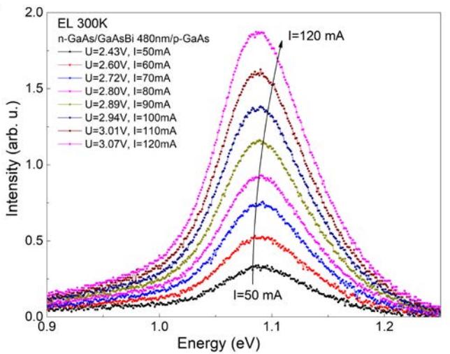
This study aims to growth technology and complex investigation of multiple quantum well (MQW) structures for LEDs exhibiting luminescent properties in spectral range from 1 µm to 1.5 µm. A new concept of LED design was proofed. Combining two earlier demonstrated by our group ideas [7, 8], pin structures with insulating layer cotaining Bi quantum dots in the wells sandwiched by parabolic quantum barriers were fabricated. The optimization of MQWs was performed by MBE, varying Bi content, QW and barrier thickness, in-situ annealing temperature and time. Photoluminescence and voltage-current measurements of MQW structures and LEDs have been carried out to evaluate the optical and electrical properties and served as a feed-back for epitaxy optimum conditions mapping. The complex characterization of samples (see Fig. 1) permitted to reveal the dominating recombination mechanisms in bismides MQWs, and define key parameters influencing to LEDs performances.