Silicon has been dominating the market of electronic and photonic devices for several decades [1]. However, mid-IR photodetectors and lasers have been recently gaining more attention due to their applicability in military, medicine and night vision and those devices require Si emission to be shifted to mid-IR. Germanium-tin (GeSn) alloy is a highly promising material for such purposes since it is compatible with silicon technology, direct energy bandgap can be achieved in this material when Sn content reaches 6-8% and GeSn absorption and emission can be shifted to mid-IR by increasing Sn content in the alloy [2]. Because of these desirable properties GeSn photodetectors, LEDs, lasers and various transistors such as MOSFETs and TFETs were created [3]. However, not all GeSn properties are well known and understood and therefore they require further research.
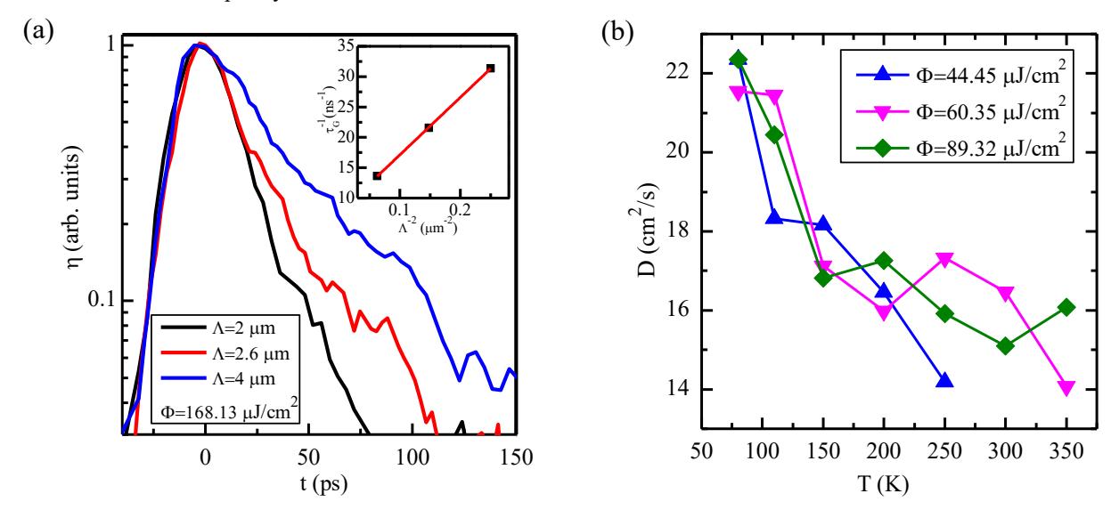
In this work carrier lifetime, diffusion coefficient and diffusion length in Ge0.95Sn0.05 epilayer grown on Si substrate were studied. These important optoelectronic parameters were determined using light induced transient grating technique. The sample was excited by pulsed laser irradiation at 527 nm wavelength which created transient grating in the layer. It caused the probe beam (1053 nm) to diffract and by using an optical delay line diffraction efficiency (${\eta}$) decays were obtained. They were measured at three different grating periods ${\Lambda}$ (Fig. 1 (a)). This allowed us to determine carrier lifetime (${\tau_R}$) and diffusion coefficient (D) using Eq. (1), while diffusion length was later calculated from these parameters. Nitrogen cryostat was used to obtain temperature dependence.
$$\frac{1}{\tau} = \frac{1}{\tau_R} + \frac{1}{\tau_D} = \frac{1}{\tau_R} + \frac{4\pi^2 D}{\Lambda^2} \tag{1}$$In Fig. 1 (b) it can be seen that diffusion coefficient decreases with temperature. It is attributed to increased phonon and defect scattering. Weak excitation dependences of the parameters are related to saturated trap regime. Also, the value of diffusion coefficient is lower than that of pure germanium $D_a = 68 \frac{cm^2}{s}$ which indicates that incorporating Sn causes worse material quality.