
The main requirements for optical coatings are low scattering losses and low absorption. Additionally, films must be deposited with precise thickness control as well as thickness uniformity. There are well known physical vapour deposition (PVD) techniques used in manufacturing optical coatings. However, due to development of laser industry, optical components are becoming increasingly complex. Examples of complex optics are photonic crystals, lenses, microoptics etc. Traditional PVD techniques are not able to achieve high-performance optical coatings on these complex substrates.
Atomic layer deposition (ALD) is a branch of chemical vapour deposition (CVD) techniques and is a promising chemical coating technology. In ALD, when depositing dielectric films, substrates are cyclically exposed to gaseous precursors which react in a self-limiting manner. This cyclic process prevents precursors from reacting in gas phase, thus the reaction is limited to the surface. The surface-controlled ALD reactions allow to control film thickness within a sub-nanometer range [1].
Optical coating design is a sequence of layers with high and low refractive indices. To manufacture simple coatings using ALD, Al2O3 could be used as a low refractive index material because thermal deposition of Al2O3 is well known and does not require a complex reactor design [2]. However, a more precise and complex optical coating design may require a higher refractive index contrast between the two layers. Silicon dioxide (SiO2) is one of the most widely used materials in manufacturing of optical coatings owing to its low refractive index and large band gap. Unfortunately, it has been shown that the deposition SiO2 using thermal process, where oxidant is water, is not sufficient [3]. Therefore, ozone and oxygen plasma were started to be used as oxidants [4].
In this work we studied SiO2 thin films deposited by ALD using tris(dimethylamino)silane and O3 or oxygen plasma as oxidant. We analysed transmission spectra in the spectral range of 190 – 980 nm of thin films deposited using different ALD process technological parameters (Fig. 1).
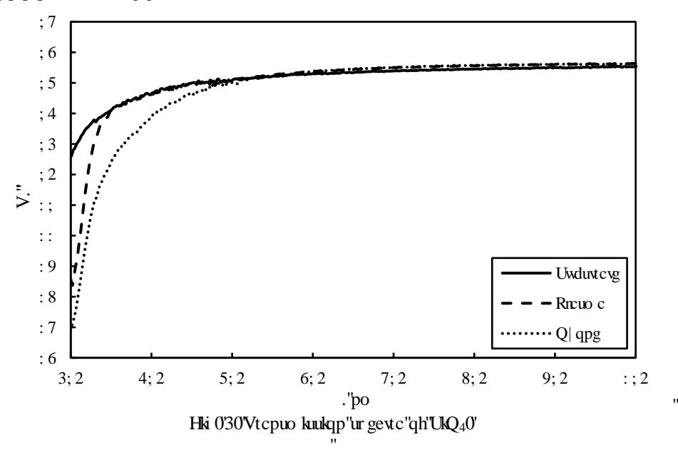
We observed different levels optical losses in UV range which were higher compared to bare fused silica substrate. To find out possible causes of absorption the investigation of chemical composition and appropriate stoichiometry of thin films using X-ray photoelectron spectroscopy (XPS) was made.