
Vertical‐External‐Cavity Surface‐Emitting Lasers (VECSELs) offer a flexible alternative to conventional Vertical‐Cavity Surface‐Emitting Lasers (VCSELs) by substituting the top distributed Bragg reflector (DBR) with an external coupler, which facilitates efficient optical pumping and provides easier access to the cavity. This architecture supports a higher output power potential, with the principal constraint of it being thermal management [1, 2].
In this study, we designed and fabricated two VECSEL chips engineered for emission in the NIR. One device with InGaAs multiple quantum wells (MQWs) in the gain region, whereas the second chip employs GaAsBi MQWs. The integration of bismuth into the GaAs lattice accelerates bandgap reduction relative to indium, while simultaneously enhancing temperature stability and increasing the spin–orbit split‐off energy, thereby mitigating non‐radiative Auger recombination and rendering GaAsBi an attractive material for long-wavelength optoelectronic applications. A sketch of such structure is presented in Figure 1 on the left, the chip can be divided in two main components, a DBR and the gain region plus window layers. Our work was focused on the optimization of the design and grown of both of these parts.
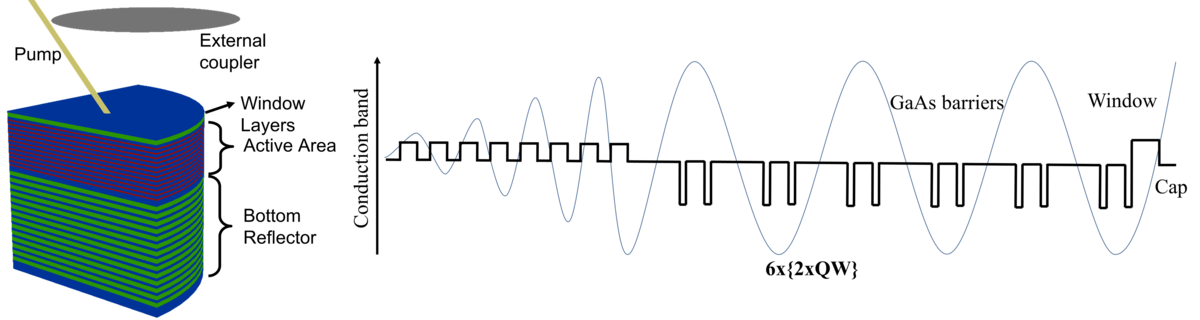
Both structures were grown by solid-source molecular beam epitaxy using a Veeco GENxplor system. A DBR composed of 30 AlAs/GaAs periods was designed to center the MQW emission within the photonic stopband. To reduce overall chip thickness and improve heat dissipation, a gain region featuring 12 quantum wells with alternating barrier thicknesses was implemented, the barrier dimensions were optimized so that the antinodes of the lasing standing wave coincide with the QW positions, thereby enhancing emission coupling, the conduction band of the full structure is presented in Figure 1 on the right, in blue the laser standing wave is shown.
Specifically, the InGaAs-based chip utilized QWs 5.7 nm thick (with 20% indium) separated by 98 nm barriers and capped with 7 nm barriers, whereas the GaAsBi device featured 5.5 nm QWs (with 8% bismuth) interleaved with barriers of 7 nm and 150 nm. Lasing was demonstrated at 976 nm from a 500 µm-diameter region in the InGaAs/GaAs device, and notably, lasing at 1070 nm was observed in the GaAsBi/GaAs device representing the first reported instance of lasing from a GaAsBi-based VECSEL. This research was funded by the Research Council of Lithuania (LMTLT), agreement No. [S-LT-TW-24-8].