Near Infrared (NIR) spectral region has a plethora of different everyday applications. Due to its high penetration depth into soft tissue, it can be used in both sensing (e.g. pulse oximetry) and treatment of humans. Furthermore, all modern communications also rely on semiconductor lasers with emission at 1300 and 1550 nm. Finally, this spectral region has a well-developed detector technology based on classical semiconductor materials (Si, Ge, InGaAs). Despite this the emitters working in this region struggle with temperature stability and due to their narrow bandgap are prone to large Auger recombination losses. More than two decades ago GaAsBi was proposed as an attractive NIR material. It has a large bandgap reduction of up to 88 meV per 1% of As being replaced by Bi in the GaAs lattice [1]. Moreover, it possesses a temperature insensitive emission spectrum, with stable room temperature operation [2, 3]. Finally, it has been showcased that the strong effect of bismuth incorporation on the valence band of the material induces a large increase of the spin-orbit split-off energy, which at 10.5 % of Bi content becomes larger than the bandgap, meaning that one of the major non-radiative Auger loss mechanisms becomes suppressed [4]. Despite these properties being direct solutions to the main drawbacks of current NIR emitters, the success of GaAsBi is limited by its complicated growth and defectiveness, stemming from the low growth temperature (< 420 \(^{\circ}\)C) and stochiometric As to Ga ratio, contrary to the classic approach in growth of AIII-BV at a group V overpressure.
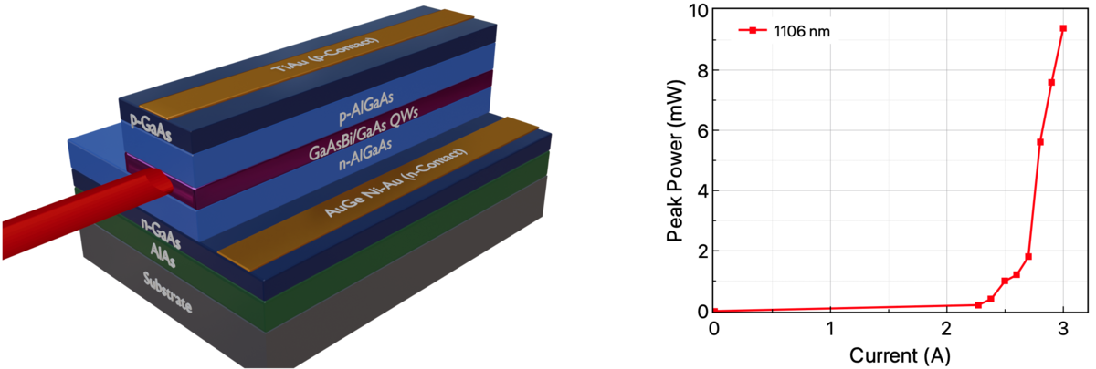
This work focuses on the MBE growth optimization of the GaAsBi active region design and fabrication of electrically pumped diode emitters. Initially, growth and characterization of GaAsBi multiple rectangular quantum well (RQW) test structures was carried out to determine the optimal growth regime and clarify the influence of parameters on the optical quality of the quantum structures. This was followed by the fabrication of laser diode (LD) and LED structures. Structures were grown with different layer designs and dopant profiles, some were additionally buffered by AlAs sacrificial layers, allowing for the removal of the substrate and bonding onto different platforms (e.g. SiC or InP). The characterization of LEDs revealed the spectral stability in a wide temperature range from 30 to 300 K, with the central emission wavelength shifting from 1035 to 1060 nm. Rapid thermal annealing was shown to have a positive influence on the LED active region quality. LDs with lasing lines in the range from 1000 nm to 1140 nm were grown and processed. The output peak power of GaAsBi 3xRQW based semiconductor microlasers reached up to 10 mW.