GaAsBi quantum well (QW) structures have gained significant interest as potential active media for optoelectronic devices operating in the near-infrared (NIR) region. One of the key advantages of GaAsBi is its strong bandgap redshift with increasing Bi content, as well as its enhanced spin-orbit splitting, which can suppress Auger recombination and inter-valence band absorption. Additionally, GaAsBi exhibits reduced temperature sensitivity, enabling tunable laser operation on a well-developed GaAs platform without the need for additional cooling [1-3].
However, the growth of GaAsBi quantum structures is challenging, as it requires low growth temperatures in order to incorporate large Bi atoms into the GaAs lattice. This leads to a high point defect density, resulting in a significant reduction in GaAsBi luminescence intensity and emission efficiency. Therefore, optimizing the growth conditions to enhance the quality of GaAsBi is crucial for developing efficient NIR sources, necessitating precise efficiency measurements, which help to fine-tune growth conditions and improve material quality.
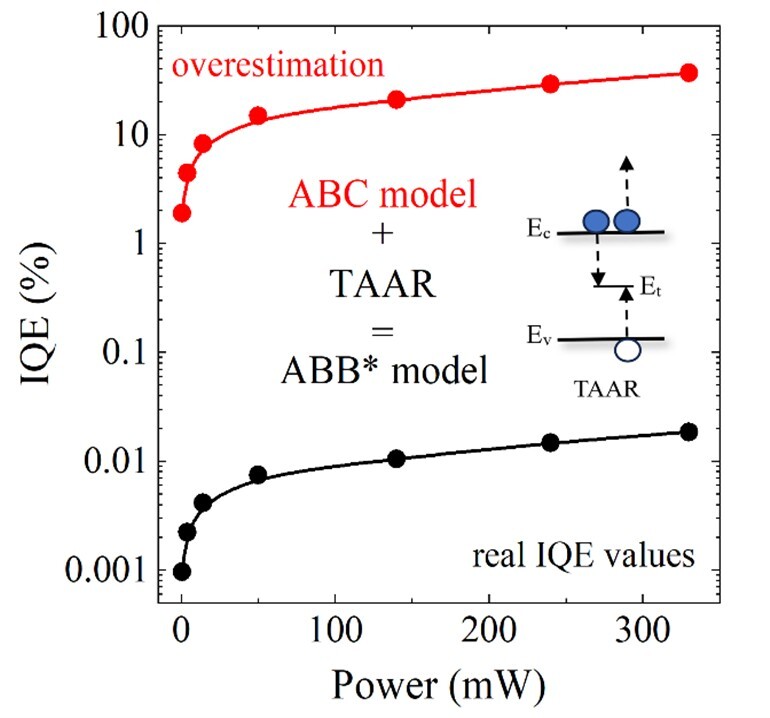
This study focuses on developing a reliable method for calculating internal quantum efficiency (IQE) of GaAsBi quantum structures. A comprehensive analysis of carrier recombination processes was conducted using absolute IQE measurements with an integrating sphere and our newly developed ABB* method [4], which includes contribution from trap-assisted Auger-Meitner non-radiative recombination (TAAR) (see fig. 1). The acquired IQE values for different quantum structures highlighted the detrimental effect of low growth temperatures and Bi content on material quality and photoluminescence (PL) emission.
We show a simple analysis method to not only calculate the IQE but also evaluate the relative carrier recombination ratios. This work facilitates a direct comparison of samples even across different research laboratories and provides valuable insights into both radiative and non-radiative recombination mechanisms. These findings contribute to the optimization of GaAsBi growth processes, paving the way for enhanced optoelectronic device performance in the NIR region.