Ferroelectric thin films are widely used in capacitors, sensors, actuators and piezoelectric microelectromechanical systems (piezoMEMS) due to their excellent dielectric and piezoelectric properties [1]. Many of these applications rely on lead-based materials for their high performance [2]. However, the environmental and health risks associated with lead have induced the search for lead-free alternatives. One of the promising candidates is 0.8Na\(_{0.5}\)Bi\(_{0.5}\)TiO\(_{3}\)-0.2BaTiO\(_{3}\) (NBT-BT) [3], though achieving high-quality thin films with controlled properties remains challenging. This study aims to optimize the deposition parameters of NBT-BT thin films grown using pulsed laser deposition (PLD) to obtain homogeneous and non-conductive materials.
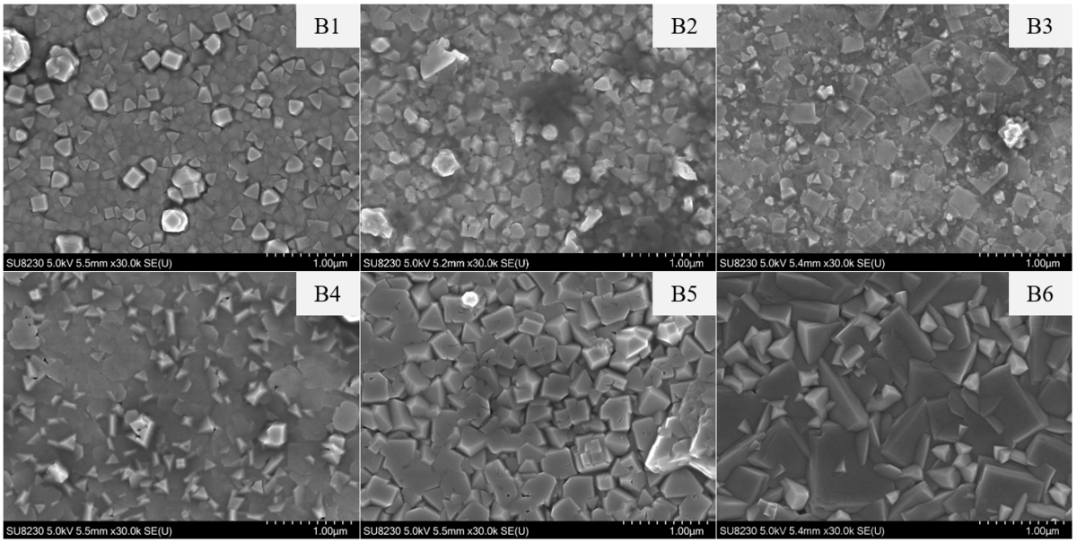
NBT-BT thin films were deposited on Pt/TiO\(_{2}\)/SiO\(_{2}\)/Si substrates using a KrF excimer laser (wavelength: 248 nm, fluence: 1.5 J/cm\(^{2}\)) at different substrate temperature, deposition distance and process pressure, as detailed in Table 1. Structural and morphological characteristics were analyzed using scanning electron microscopy (SEM) and X-ray diffraction (XRD). Dielectric properties were measured using an LCR meter to examine ferroelectric properties. The obtained results indicate that deposition parameters significantly influence crystallinity, grain size, and film uniformity which can be seen in Fig. 1. A well-defined perovskite phase was observed under optimized conditions.
These findings highlight the importance of parameter control in PLD for fabricating high-quality NBT-BT films on silicon and platinum substrates. The study provides insights into optimizing deposition conditions for improved film uniformity and electrical properties, contributing to the advancement of lead-free ferroelectric materials for future usage in electronic devices.
| Sample | Temperature, \(^{\circ}\)C | Process Pressure, mbar | Distance, mm |
|---|---|---|---|
| B1 | 600 | 0.3 | 55 |
| B2 | 600 | 0.3 | 75 |
| B3 | 600 | 0.3 | 95 |
| B4 | 550 | 0.3 | 55 |
| B5 | 650 | 0.3 | 55 |
| B6 | 600 | 0.06 | 55 |