Crystalline silicon (c-Si) solar cells are very popular due to their low cost and relatively good efficiency. However, the reduction of optical losses which are mainly attributed to reflectance is still one of the technological challenges in achieving higher efficiencies [1].
In this work, a 200 nm chrome thin film was deposited on a polished Si wafer by e-beam evaporation technique. The purpose of chrome film was to act as a mask for the reactive-ion etching process of the silicon substrate. Then, laser-induced periodic surface structures (LIPSS) were imposed on the surface via femtosecond laser Pharos (Ligh conversion), at 200 kHz and 1030 nm wavelength. Fluence varied in range from 147 to 245 \(mJ/cm^{2}\). Then, quazi-periodic structures were thinned down in chromium etchant (Sigma Aldrich) solution for 40 s to expose the silicon surface. Later, the inductively coupled deep reactive-ion etching process was applied to transfer a grating-like structure mask from chrome into the crystalline silicon substrate. Lastly, we used the same chromium etchant to completely remove the chrome mask.
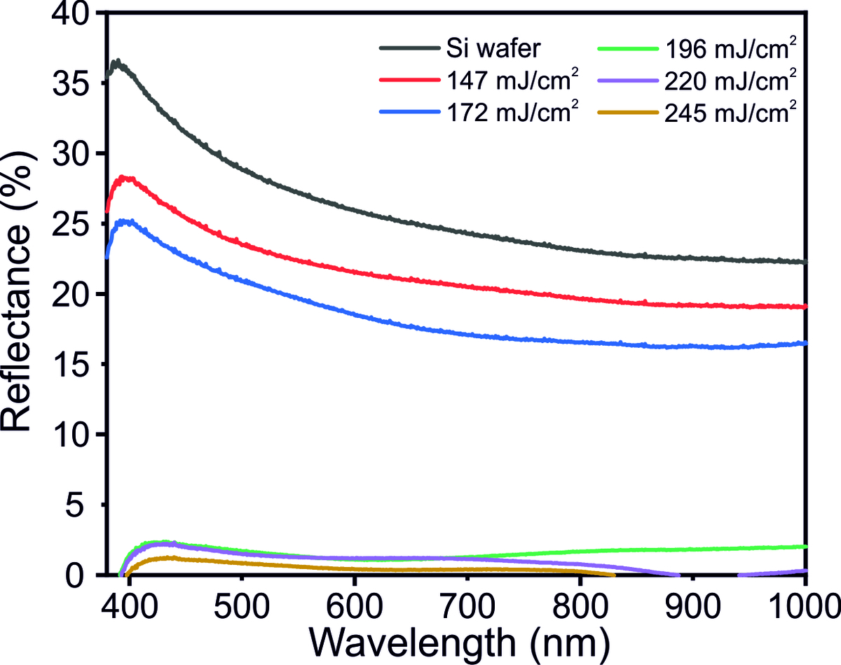
Reflectance measurements in UV-Vis-NIR with integrating sphere were performed for pristine and laser-treated surfaces. The 28 % reflectance of the pristine Si wafer was reduced by 23 and 20 % by applying 147 \(mJ/cm^{2}\) and 172 \(mJ/cm^{2}\) fluence irradiation and imposing the LIPSS (Figure 1). An even bigger drop in reflectance was obtained when 196, 220, and 245 \(mJ/cm^{2}\) fluence was used, where it went below 2 %.
Our work shows that LIPSS in chrome thin film can be used as a mask for silicon etching and formed structures greatly reduce reflectance.