Widely studied for its exceptional electrical, thermal and optical properties, graphene is a promising material for electronic and optoelectronic device applications. Among these, graphene-Si Schottky junctions are actively researched for their potential use as solar cells, gas sensors, photodetectors and barristors [1]. However, the graphene-Si junction presents unresolved challenges including large variation of the ideality factor (~1-30) and limited performance due to graphene-Si interface defects such as dangling bonds at Si surface [2]. In effort to mitigate the latter problem passivating insulator layer is introduced between Si and graphene, with hexagonal boron nitride (h-BN) being well-suited due to its close lattice match to graphene [3]. To investigate such junctions low-frequency noise measurements are employed as they have proven to be a sensitive tool for assessing device quality, defectiveness and reliability and provide insight into underlying physical processes. The aim of this work is to investigate the low-frequency noise characteristics of graphene/h-BN/n-Si(100) junctions for evaluation of their overall performance and its dependence on h-BN layer thickness.
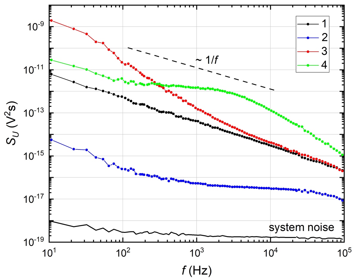
Graphene/h-BN/n-Si(100) junctions with different h-BN layer thicknesses (0-15 nm) were investigated. Graphene was directly synthesized on the substrate using microwave plasma-enhanced chemical vapor deposition (PECVD). Electrical noise characteristics were measured in the 10 Hz – 100 kHz frequency range at forward and reverse bias. In all investigated samples 1/f or 1/f \(^{\alpha}\)-type fluctuations were observed with “white” spectrum part of thermal noise at low bias (Fig. 1). Several samples are distinguished by Lorentzian type spectra (samples 3 and 4 in Fig. 1), which are attributed to charge carrier capture and emission processes with distinct relaxation times. Samples with higher resistance showed higher noise intensity while samples with the greatest h-BN layer thickness (15 nm) are characterized by lower noise intensity.