
Indium gallium arsenide (InGaAs), a III-V group semiconductor alloy of indium arsenide (InAs) and gallium arsenide (GaAs), is valued for its tunable bandgap, high electron mobility, and enhanced quantum confinement effects [1-2]. These properties make it crucial for applications in photonics, high-speed electronics, and telecommunications [3-6]. The main drawback of the material is that the lattice mismatch between InGaAs and its GaAs substrate causes strain and defects like dislocations [7], which degrade performance by reducing carrier mobility and affecting optical properties [8]. In order to address this challenge, the growth parameters have to be optimized. In this work the InGaAs quantum structures were studied by performing photoluminescence (PL) measurements at different wavelengths to assess how growth parameters affect their structural properties.
Four InGaAs samples with varying In content (from 18% up to 26%) and structural features (barrier thicknesses) were grown by molecular-beam epitaxy (MBE) and investigated using a confocal microscope system. PL measurements using lasers with 405 nm and 662 nm wavelengths probed the structures at different depths to examine emission characteristics and assess material homogeneity.
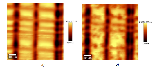
The study found that emission maps differed significantly based on excitation wavelength due to variations in penetration depth. Defects visible with shorter excitation wavelengths were undetectable with longer wavelengths (Fig. 1). The results showed that indium content influences spectral properties, with higher indium levels leading to broader, red-shifted spectra under longer wavelength excitation. However, inconsistencies were observed under 405 nm excitation, likely due to limited penetration depth and noise.
The obtained results suggest that indium content has direct impact on the spectral width and shift of the material‘s emission spectra. In addition, linking the features observed with different excitation wavelengths with the structural properties requires accurately determining absorption coefficients at energies significantly above the band gap.