
Radiation-induced transformations of boron dopant in p-type silicon (Si) lead to the “acceptor removal”, which degrades the performance of particle detectors [1]. The effect arises due to the transformation of substitutional lattice site boron (B\(_{s}\)) into interstitial (B\(_{i}\)) boron under irradiation. The subsequent migration of B\(_{i}\) and its interaction with interstitial oxygen impurity (O\(_{i}\)) in the Si crystal result in the formation of the interstitial boron–interstitial oxygen complex (B\(_{i}\)O\(_{i}\)), further altering the material properties. Alternative materials, such as silicon-germanium (SiGe), are being researched to mitigate these issues. SiGe alloys are promising materials for applications in photovoltaics, space technology, and high-frequency heterojunction bipolar transistors operating in the near-THz range [2]. Recent studies suggest their potential use in lithium-ion battery anodes [3] and microelectronic/optoelectronic devices, including high-speed temperature sensors, Hall-effect transducers, and γ-ray detectors [4,5]. In this work, p-type silicon (Si) and SiGe diodes with different Ge contents irradiated with 5,5 MeV electrons were studied. Capacitance deep-level transient spectroscopy (C-DLTS) and photoionization spectroscopy (PIS) were used to observe radiation-induced defects in SiGe detectors.
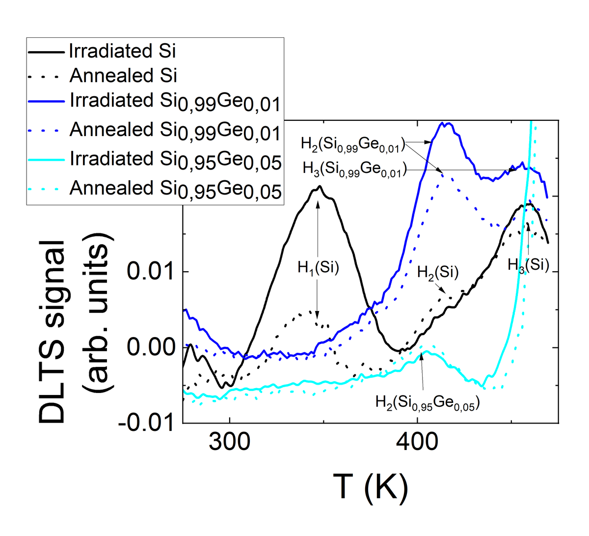
The DLTS spectra were measured in the 15–475 K temperature range. The spectra of the majority carrier traps were recorded at a reverse bias voltage of -5 V (U\(_{R}\)) and injection pulses of 200 ms duration (tp) at -0.1 V (U\(_{P}\)) (Fig.1). The spectra of the minority carrier traps were also investigated at reverse bias voltage (U\(_{R}\)) of -1 V and injection pulses of 200 ms duration (tp) at 2 V (U\(_{P}\)).
The results of this study, highlighting the radiation-induced defect dynamics in p-type Si and SiGe diodes with varying Ge contents and their evolution under annealing, will be presented and discussed in detail.