Thin-film solar cells have the potential to become the future of solar energy, as their production requires fewer materials, and their efficiency is rapidly approaching that of currently used solar cells. One of the materials used in the fabrication of thin-film solar cells is antimony selenide (Sb₂Se₃) [1]. This semiconductor, characterized by a one-dimensional crystalline structure, has a band gap of approximately 1.2 eV, an absorption coefficient exceeding 10⁴ cm⁻¹, and electron mobility in monocrystals ranging from 10 to 40 cm²V⁻¹s⁻¹. Due to its structural properties, the electrical characteristics of the semiconductor’s surface vary depending on the grain orientation, which may influence charge transport in Sb₂Se₃ heterojunctions [2,3]. In this work, we aim to investigate how ionization potential changes with Sb₂Se₃ grain orientation and how it affects the charge carrier transfer.
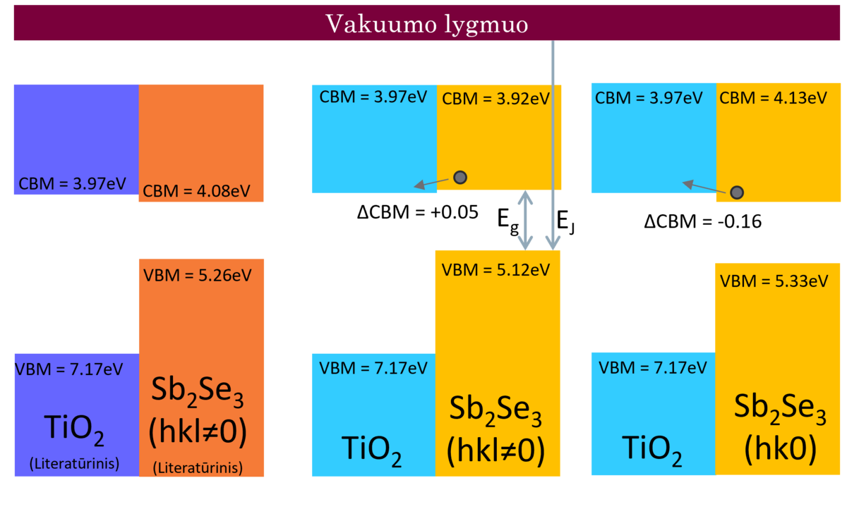
To determine the energy band alignment in the heterojunction with titanium oxide (TiO₂), X-ray photoelectron spectroscopy (XPS) and ultraviolet photoelectron spectroscopy (UPS) were utilised. Three Sb₂Se₃ samples with different grain orientations were studied: (hkl) with l ≠ 0, (hk0), and (120). The XPS method, together with Ar etching, was used to identify chemical elements and to get rid of contaminants. UPS was utilised to analyse valence electron spectra, from which semiconductor ionization energy (E\(_{J}\)) corresponding to the valence band maximum (VBM) was determined. The energy band structure was developed using the obtained VBM values and the literature-reported Sb₂Se₃ band gap (E\(_{g}\)). E\(_{J}\) and E\(_{g}\) of TiO₂ were taken from the literature and were used to illustrate band alignment in the heterojunction.
The calculated VBM positions for the (hk0) and (120) samples were very similar (approximately 5.3 eV), while for the (hkl) orientation, where l ≠ 0, the value was 5.1 eV. By constructing the heterojunction energy band diagram, the conduction band minimum (CBM) positions of Sb₂Se₃ were determined. For the (hk0) orientation, the CBM offset in the heterojunction was -0.16 eV, whereas for (hkl) with l ≠ 0, the offset was +0.05 eV. This suggested that charge carrier transfer across the TiO\(_{2}\)/Sb\(_{2}\)Se\(_{3}\) (hkl, l≠0) heterojunction is more favourable than in TiO\(_{2}\)/Sb\(_{2}\)Se\(_{3}\) (hk0) because of lower energetic barrier for electrons. As such, higher Sb\(_{2}\)Se\(_{3}\) solar cell performance usually observed in thin films with (hkl, l≠0) grain orientation originates not only because of higher carrier mobility, but also because of more efficient charge carrier transfer across the heterojunction.