
Today lasers are used in many fields, particularly in optical fiber communication, optical digital recording, material processing, biology and medicine, spectroscopy, imaging, entertainment, and many others. Increasing demand of exceptional investigation conditions studying various materials require unique set of laser parameters - emission wavelength, its tunability, beam quality, operation temperature, optical output power. Herewith, convenient method of laser excitation, power consumption, high-speed modulation and device size become very important factors.
Vertical-external-cavity surface-emitting lasers (VECSEL), also called optically pumped semiconductor lasers or semiconductor disk laser belong to relatively new laser family that combines many of the desirable properties. In comparison to both types of electrically pumped, vertical-cavity surface-emitting lasers (VCSEL) emitting low power circular fundamental transverse mode beam and edge emitting lasers (Fabry-Perot and DFB) reaching high output power but exhibiting asymmetric beam with strong angular divergence, VECSELS are capable to generate high optical power beam keeping high circular quality [1-3].
In this work the behaviour of the emission wavelength was studied in relation to the design parameters of the VECSEL chip.
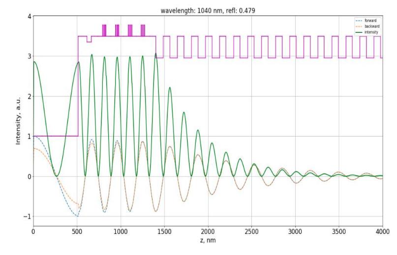
Modelled VECSEL structure is demonstrated in Fig.1. To obtain lasing it is necessary to design the Bragg mirror, gain region and surface barrier layer (window) depending on the target wavelength of the laser. The gain region is usually composed from quantum well structure calculated to match the laser optical standing wave antinodes as shown in Fig.1 (green curve).
Multiple InGaAs/GaAs quantum wells (MQWs) and AlAs/GaAs Distributed Bragg reflector (DBR) were used for VECSEL architecture. The separate layers and VECSEL structures were grown using solid-source MBE system (Veeco GENxplor R&D) equipped with standard cells for metallic Al, Ga and unique As design source generating pure arsenic dimers flux. The structure was grown on semi-insulating GaAs substrate oriented in (001) crystalline plane. To balance strain of QW in the laser structure, QW width d and In content was varied. In content in the QW was changed from 5% to 30%, thickness of QW was ranged between 3 nm and 8 nm. The emission wavelength of grown multiple quantum wells and VECSEL structures was measured using photoluminescence spectroscopy at wide temperature range of 300 K - 4 K. The quality of DBR in spectral range from 800 nm to 1500 nm was tested using ellipsometer.
After detailed study of In content and QW thickness influence to the optical properties of MQW, the complete chip was fabricated, aiming at the production of a VECSEL demonstrating emission wavelength of 976 nm. The reflectance of DBR was modelled for 25-30 GaAs and AlAs periods to obtain higher than 97% at central DBR wavelength of 976 nm. The number of InGaAs MQWs was optimized to 12. The active area of structure was covered by 165 nm thick-AlAs window and 5 nm GaAs capping layer. The results of Reflectance and Photoluminescence measurements and characterization by Atomic Force Microscopy of grown layers and VECSEL structures will presented.