Gallium nitride (GaN) is a widely used material in many optoelectronic applications due to its direct band gap, high breakdown voltage and high electron mobility. However, GaN growth on foreign substrates deteriorates its crystalline quality due to the lattice constant and thermal expansion differences. The solution to this problem would be the use of native substrates. Yet, bulk GaN substrates are relatively pricy and come in limited size. To tackle these problems, graphene interlayers could be used [1]. In the process called remote epitaxy, GaN formation is governed by its interaction with the GaN substrate through monolayer graphene. The seeding effect of the substrate enables high quality GaN growth, while weak van der Waals interaction facilitates subsequent layer release and the reuse of an expensive substrate. In addition, this growth method enables production of flexible GaN films, which can be used for novel applications. It is essential to examine interlayers quality and thickness. It was shown that graphene surface treatment has an impact on subsequent GaN formation [2].
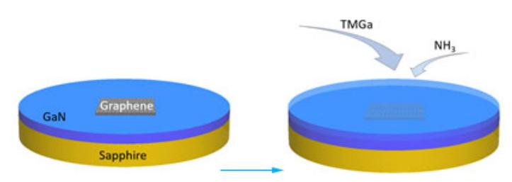
In this work, metalorganic chemical vapour deposition (MOCVD) was used to grow GaN epilayers on the single-layer graphene covered GaN/sapphire templates (see schematics in Figure 1). Commercially available, transfer-ready monolayer graphene with PMMA support was wet-transferred to partially cover the templates prior to the MOCVD growth. The quality of graphene was evaluated by Raman shift. Particular attention to the graphene treatment temperature prior GaN deposition was given. GaN layers of different thickness were grown and investigated using XRD, AFM and PL techniques.
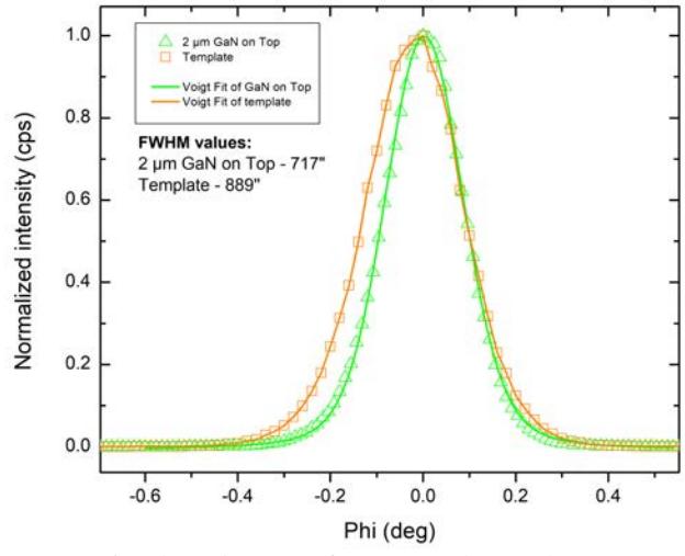
X-ray diffraction scan of (1 0 \bar{1} 0) plane GaN revealed crystalline quality improvement over the GaN template. The crystalline quality improvement is presented in the Figure 2.