
SiGe material based devices are capable to operate in the radiation harsh environment and it had been demonstrated that SiGe alloys are prospective for fabrication of $\gamma$-ray detectors [1]. Cadmium zinc telluride (CZT) is a promising material for the room-temperature X- and $\gamma$-ray detectors due to high average atomic number providing high stopping power as well as rather large band-gap which determines large resistivity, small leakage-current, and good energy resolution [2]. Generation of the undesirable point defects is inevitable during crystal growth and operation of detector in radiation harsh environment. The dopants, native impurities and radiation induced defects usually act either as recombination, trapping or carrier emission centres and contribute to the decrease of charge collection efficiency by reducing carrier lifetime. The role of point defects is also important in charge compensation processes. Therefore, the analysis of defects is important in prediction of the optical and electrical characteristics of the SiGe and CZT materials. In this work, study of pristine, 5.5 MeV electron and 1.6 MeV proton irradiated Si1-xGex structures, containing 1% and 5% of Ge, and two sets of CZT samples, exhibiting good and unacceptable performance of radiation detection, have been performed by combining techniques of the microwave probed photoconductivity (MW-PC) and pulsed barrier evaluation by linearly increasing voltage (BELIV).
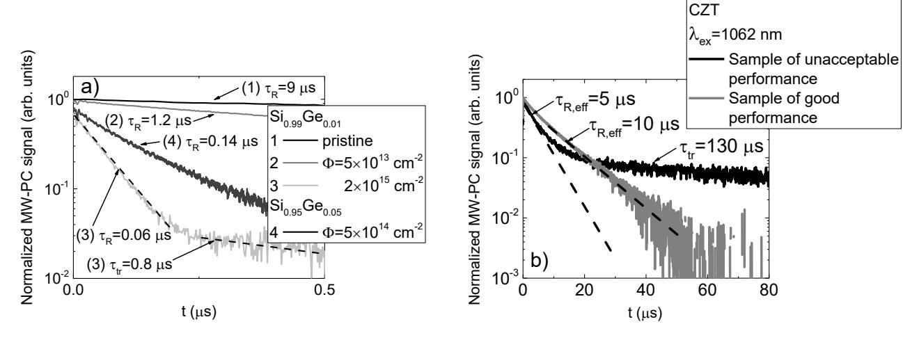
It has been revealed that in SiGe material both carrier recombination and trapping lifetimes decrease near-reciprocally (Fig. 1a) relative to the density of radiation defects acting as carrier capture and thermal emission centres, with predominance of point radiation defects. It has been hypothesized that the single-type deep centres are involved in both carrier photo-generation and thermal emission processes. Activity of point defects can be modified by anneal procedures, and sensor functionality can be recovered (at least, partially).
The main difference between the examined CZT diodes appeared through carrier trapping effect, observable only for diodes exhibiting unacceptable performance of radiation detection (Fig. 1b). The rather long instantaneous trapping lifetime of $\tau_{tr} = 130~\mu s$ showed the trapping coefficient to be of the order $K_{tr} = 27$. The concentration of trapping centres has been estimated to be $> 3\times10^{14}~\rm cm^{-3}$ for the shallowest thermal emission centres. These trapping centre concentrations exceed dopant density by several orders of magnitude. The trapping centres in CZT material might be associated with TeCd as well as VCd point defects and Te inclusions.