
Sculptured thin film technology allows to produce nanostructured coatings featuring various properties, like certain porosity and anisotropy [1]. By optimizing these and other parameters, one can obtain coatings with different optical characteristics, which can be adapted for optical element realization. Furthermore, these coatings possess excellent resistivity to laser irradiation when silica material is used and can be deposited directly onto microlaser system components [2]. Therefore, this technology is a potential research area for microlaser component manufacture.
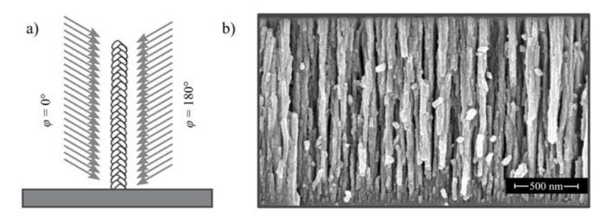
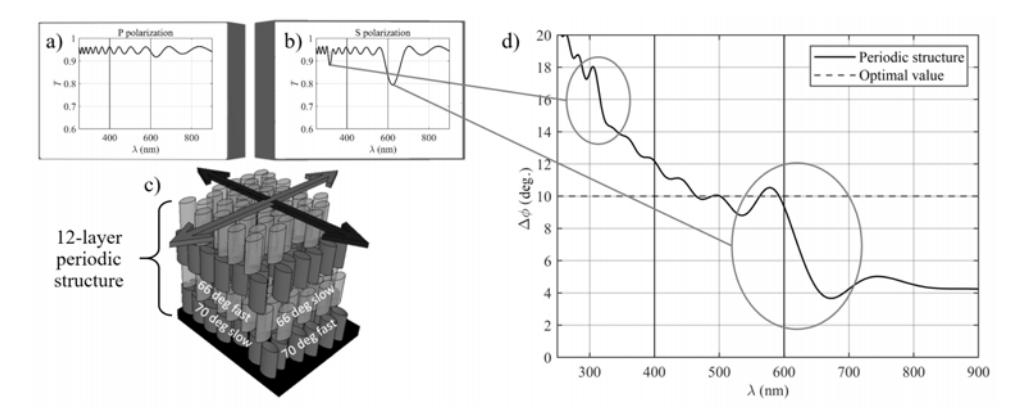
In this work, however, the scope of investigation was limited to achromatic waveplates. Thus, the main objective was to examine the optimization and manufacture potential for sculptured thin film based achromatic waveplates. The problem was approached by utilizing anisotropic properties of serially bideposited (see Fig. 1) orthogonally birefringent SiO2 multilayer structures (see Fig. 2). Due to the existence of unique Kramers-Kronig relations for transmission amplitude coefficient $\tau$ [3], different transmittance T band-gaps for S and P polarised radiation result in corresponding phase shift differences, which allow to compensate for natural dispersion (see Fig. 2). Taking full advantage of this mechanism, achromatic waveplate designs were optimized employing Dlib global optimization C++ library routines [4].
The main source of error in manufactured waveplate optical and phase characteristics was determined to be caused by inaccurately chosen birefringence values and deposited layer thickness errors, which reached 7.5%. Nevertheless, the examination of a more robustly designed waveplate allows to conclude that with accurately chosen birefringence values a functioning achromatic waveplate can be successfully manufactured.