Semiconductor quantum dots (QDs) have attracted considerable research interest in recent years due to their distinct properties. These nanostructures have shown a number of advantages over bulk and quantum well structures, which are commonly used as gain media in photonic applications [1]. Given the growing interest, bismuth (Bi) QDs have emerged as a promising candidate for optoelectronic devices operating in the near-infrared (NIR). The formation of Bi QDs was first described by Luna et al. [2], where GaAsBi was subjected to post-growth thermal annealing. While bulk Bi is semimetallic, theoretical estimates predicted that Bi nanoparticles become semiconducting at diameters below 16 nm [3]. Emission from Bi QDs in the wavelength range of 1300–1500 nm was reported in the same work, however, no further optical studies of Bi QDs have been conducted.
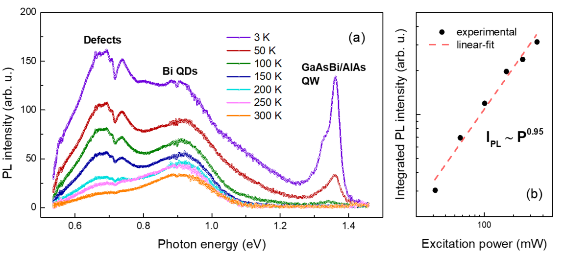
In this work, we present a comprehensive photoluminescence (PL) study of Bi QDs to understand how growth and annealing conditions impact their optical properties. Various GaAsBi/AlAs quantum well (QW) heterostructures with thicknesses of 4 and 10 nm were deposited by molecular beam epitaxy at substrate temperatures ranging from 165 to 330 °C. A rapid thermal annealing (RTA) oven was used for post-growth annealing at temperatures above 650 °C. It was demonstrated that after thermal treatment a broad band centered around 0.9 eV, related to emission from Bi QDs, emerged in the room temperature PL spectra. The bismuth nanocrystal peak for the 10 nm-thick GaAsBi/AlAs QW structures was redshifted when compared to that of the 4 nm, indicating that larger QDs form in wider QWs. Temperature-dependent measurements in the 3-300 K range revealed good thermal stability of the Bi QDs band gap (Fig. 1a). Moreover, excitation-dependent PL measurements at room temperature (Fig. 1b) suggested that Bi clusters exhibit strong carrier confinement effects, comparable to quantum dots grown by the Stranski-Krastanov method [4].
These findings imply that with further optimization of growth and annealing conditions, GaAsBi QWs containing bismuth QDs could be a promising material for devices operating in the NIR spectral range.