Our daily lives are packed with many integrated, functional, and miniaturized devices, the demand for which has increased significantly in recent years. Among the most widely used electromechanical sensors are piezoresistive, a type of pressure sensor based on the piezoresistive effect. This effect describes how the electrical resistance of a material changes when it is subjected to a mechanical load. Piezoresistive sensors are widely studied due to their excellent sensitivity, simple design and durability. Their advantages are their relatively low cost of production, the possibility of obtaining different sensitivities and the wide range of measured pressures.
The integration of flexible dielectric materials is a necessary factor for the development of flexible and miniaturized electronics. To achieve this integration, it is necessary to develop technologies to create electrically conductive zones on the surface of dielectrics. The effective use of such materials requires technologies that allow the localization of such zones with high precision.
In this work, widely used engineering polymers polyimide (PI) and polyetherimide (PEI) are investigated. PI and PEI are high-temperature polymers with outstanding thermal and dimensional stability, chemical resistance, and good electrical properties. These polymers are widely used in aerospace, automotive and consumer products. [1] However, further research into selective surface metallization and electrically conductive zone formation technologies is needed for their successful application in integrated electronics. Selective surface activation induced by laser (SSAIL) has been chosen as the metallization technology to form conductive copper traces. As a possible technology for forming sensitive areas of the sensor, laser-induced graphene (LIG) technology was chosen.
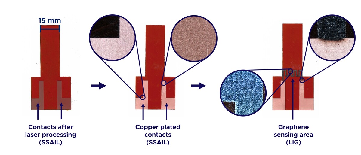
It has been experimentally demonstrated that a 3.3 kΩ piezoresistive sensor with a LIG layer on a polyimide surface can be fabricated by combining different laser technologies (Fig. 1). Such a methodology has great potential and can be used as one of the alternative and sustainable solutions for the production of flexible sensors with integrated electronics. However, further research is still necessary to improve the stability, repeatability, and efficiency of the resistance response of the LIG layer. The properties of the junction between graphene and copper also need to be improved to minimize the junction resistance. For this purpose, further optimization of the LIG process will be carried out by tuning the laser process parameters, exploring different designs, and further analysis of the contact formation between copper and graphene.