
Femtosecond Laser Two-Photon Polymerization (FLTPP) fabrication is non-linear Direct Laser Writing (DLW) lithography technology [1] which explores new areas in micro/nanometer scale fabrication and high quality 3D structuring capabilities of microoptical components [2, 3]. Due to simultaneous Two-Photon Absorption (TPA) ultralocalized photochemical reaction is initiated in the bulk of the photopolymer. Complex geometry true Three Dimensional (3D) structures with the sub 100 nm spatial resolution [4] can be point-by-point directly written in the photopolymer from Computer Aided Design (CAD) models and thus the architecture of the structure can be changed flexibly. The integrity of the FLTPP technology opens possibilities to fabricate microstructures on various substrates such as glass, plastic or metal [5].
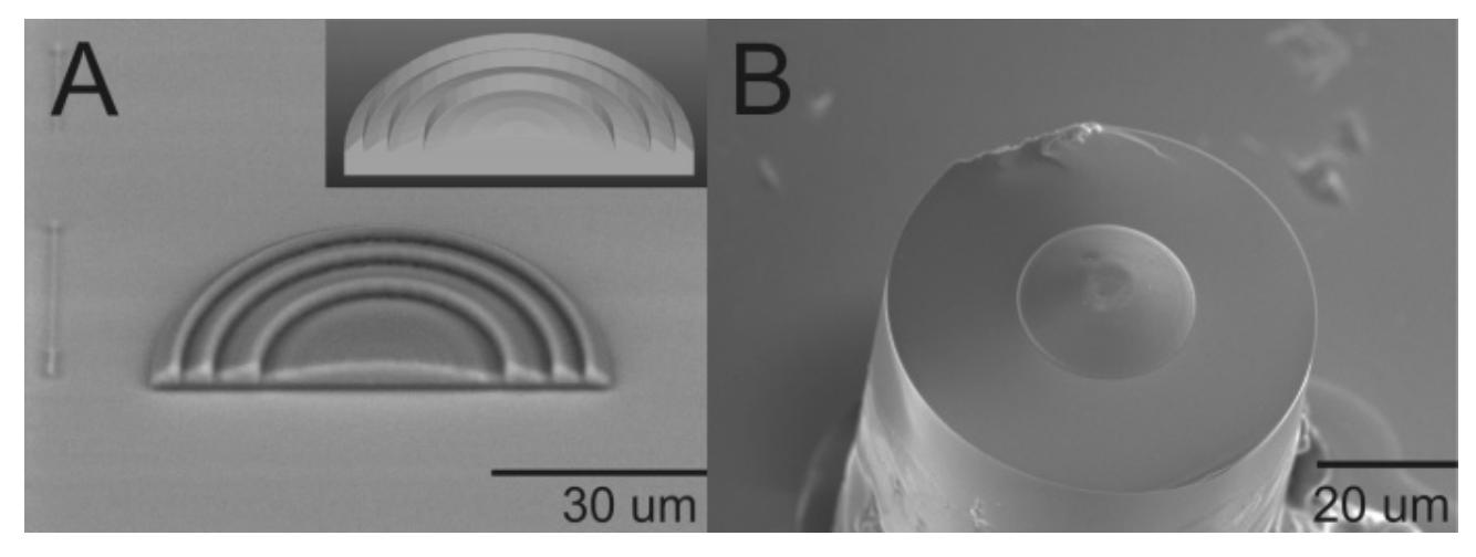
In this report, we present micro-optical components fabricated on the top of the optical fiber out of commercially available hybrid zirconium-silicon containing photopolymer SZ2080 (FORTH, Crete, Greece) [6]. The structural quality and surface roughness of the lenses were investigated by Scanning Electron Microscopy (SEM) and Atomic Force Microscopy (AFM). The optical focusing characteristics of the lenses fabricated on the glass substrate and on the top of the fiber were measured and compared with theoretical calculations. The principal setups of the FLTPP and methods of focal lengths' measurement have been described previously elsewhere [7]. The obtained results show possibility to integrate micro-optical components on the top of the fiber and use it for creation of 3D optical circuitries.