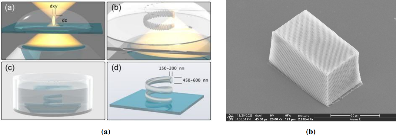
Two photon lithography is a Laser Direct Writing technique (DLW) that allows high precision 3D micro and nano-structures manufacturing with sub-diffraction-limit resolution. Thanks to the advent of femtosecond lasers, nonlinear light-matter interactions are achievable by focusing such high intensity beams into the photo-resins, which due to temporal and spatial overlap can result in two- or even multi-photon absorption inside the volume of the tightly focused laser beam, allowing to polymerize the material in a small confined region, Fig. 1a. This significant advantage makes it a suitable and high desirable technique for the fabrication of micro and nanoscale 3D structures, and it’s been widely employed for applications in several fields such as microelectronics, microfluidics, life sciences or photonics.
In this work we explored one of these applications: the fabrication of a 3D photonic crystal, Fig. 1b, able to slow down while spatially separating the frequency components of the light, which results in a localized increase of light intensity chromatically resolved, and thus can be used for application in which enhanced light-matter interaction is required, like optical sensors, solar cells or night vision devices.