The first discovery of p-type gallium nitride (p-GaN) grown by metalorganic vapor phase epitaxy (MOVPE) and doped with magnesium (Mg) was made by Japanese researchers by exposing the crystal to a low-energy electron beam [1]. The primary advancement in p-type GaN technology has been achieved through thermal annealing in a nitrogen atmosphere, which effectively activates the Mg acceptors by removing hydrogen. Hydrogen is known to passivate Mg by forming complexes that prevent Mg from effectively accepting electrons, thus hindering its p-type doping capabilities. However, defects such as nitrogen vacancies can compensate for the p-type GaN during growth. Despite this, the commercial significance of p-type GaN is considerable, although some challenges remain in understanding and optimizing the growth process.
In the technology for growing III-group nitride crystals, indium (In) can be part of the InGaN alloy and surfactant component. It has been demonstrated that In enhances the surface morphology of GaN, reduces deep-level trap concentrations, increases luminescence efficiency, extends free exciton recombination time, and improves hole conductivity [2]. This study will demonstrate that using In as a surfactant also alters the contact resistance.
We grew p-type GaN samples in an MOVPE reactor and varied parameters such as temperature and the flow rates of Mg and In metalorganics. We adjusted the In flow rate to assess the contact resistance while keeping other parameters stable. Initially, we used MICROTECH LaserWriter photolithography to pattern a photoresist layer with the geometric design of the photomask. We deposited Ni/Au contacts onto the patterned areas in an electron beam evaporation (EBE) chamber. Finally, we calculated the contact resistance by measuring the IV characteristics and using the transmission-line matrix (TLM) method.
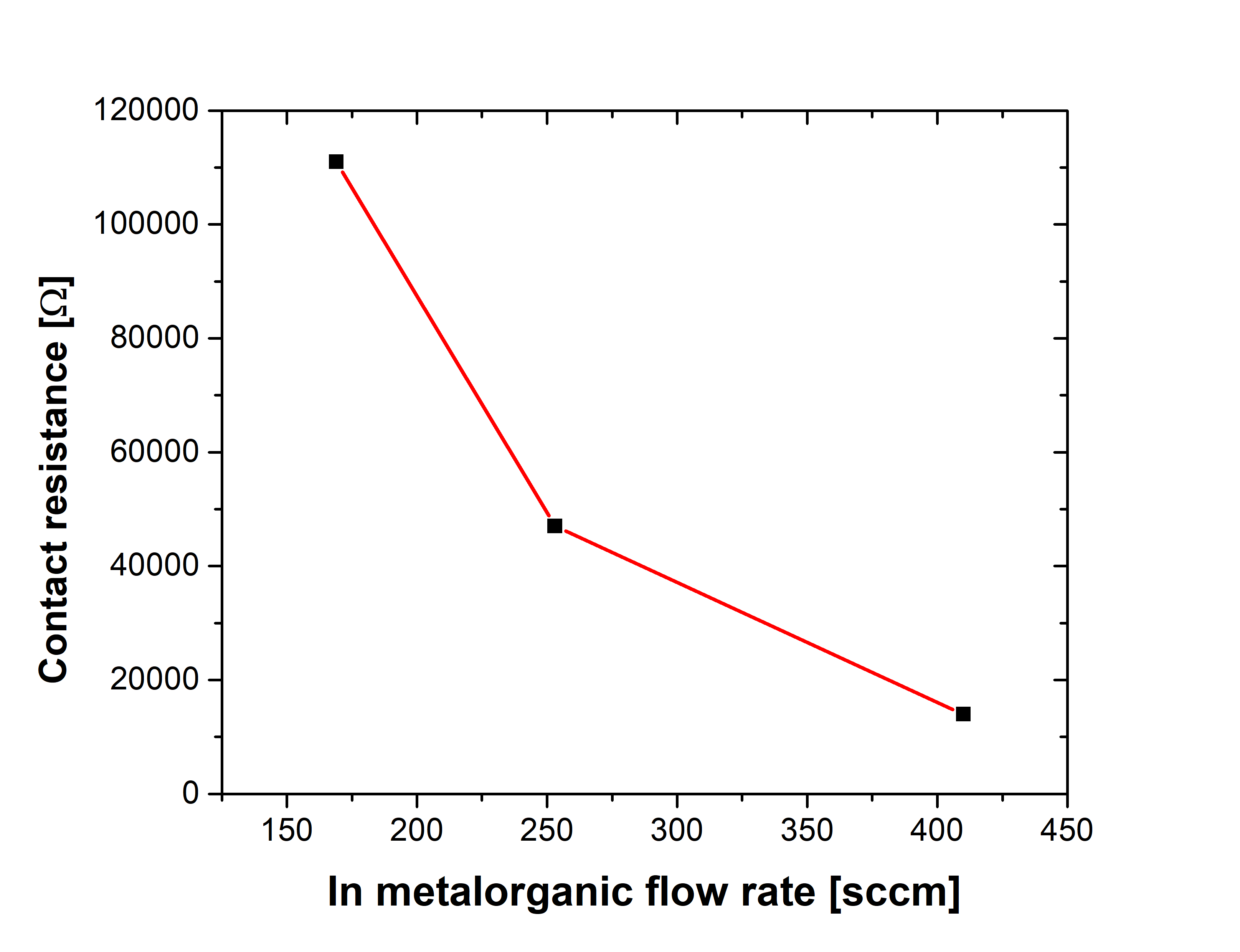
To summarize the experimental findings, we observed that the In surfactant influences the contact resistance. We found that as the In concentration increases, the contact resistance decreases (Fig. 1). Furthermore, the In surfactant increases the carrier diffusion length.