
Laser annealing is a promising method to boost photovoltaic device performance by affecting semiconductor material properties. The use of lasers provides precise control over energy delivery and spatial distribution, allowing modifying materials characteristics locally. Achieving uniform effects over the surface requires a nuanced approach, as there is no one-size-fits-all method. In this work, we used a nanosecond pulsed 532 nm wavelength laser. We explored two different strategies to anneal samples of antimony selenide. The first approach was to heat sample using a single laser beam and by changing filters, exposure time and frequency of the laser to simulate different annealing conditions. Another strategy was to focus laser beam and scan on the designated area on the sample. The scanning of the laser beam was realized using galvanometric mirrors. Various mirror control and laser parameters were tested to achieve uniformly annealed areas on the sample. To get the results, we went through several important steps. We started with using a single large laser beam, which posed challenges with non-uniform absorption within a 700-micrometer diameter for annealing our photovoltaic samples. Seeking improvement, we experimented with scanning and introduced a diaphragm and galvanometric mirrors. However, the scanning beamś size led to uneven surface coverage. Recognizing the need for uniformly affected areas, we refined our approach by using a long focal length lens which contracted the beam’s size to 160 micrometres and adjusting the parameters of the mirrors to achieve uniform coverage. This method allows for precise adjustments of the mirrors to accommodate variations in material or laser parameters, ensuring consistent and uniform impact on laser-irradiated surface areas. Importantly, the transition from a single beam to scanning resulted in an increase of affected area, expanding from 1 mm² to 25 mm². Nevertheless, our final setup encountered challenges, including uncovered areas caused by synchronized frequencies in laser and scanning settings, along with variations in thermal excitations that affected the scanning path width. However, through galvanometric mirror parameter adjustments, we effectively solved these problems, identifying optimal parameters for accurate scanning. The visual evidence from images (Fig. 1, a)) depicting uniform coverage solidifies the success of our approach. In conclusion, our laser annealing system achieves uniform coverage on samples, enhancing photovoltaic device performance. Moreover, it presents a potential alternative to moving-stage laser annealing systems. Its adaptability allows for the use of different lasers and samples, offering versatility and potential for optimizing material properties.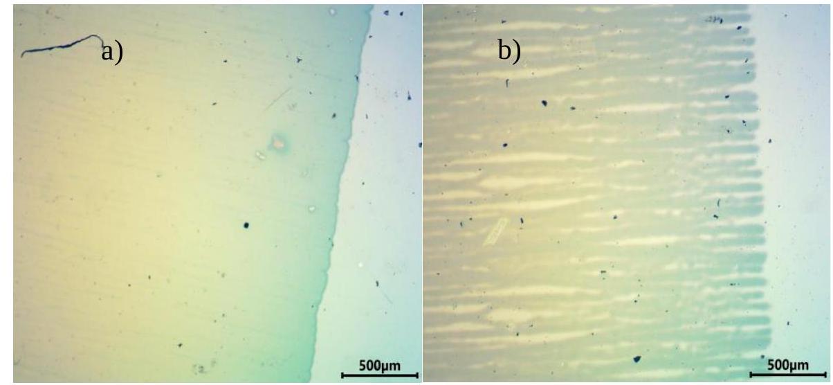
OPTIMIZING PHOTOVOLTAIC DEVICES THROUGH GALVANOMETRIC MIRROR-ASSISTED LASER ANNEALING
Gustas Mickevičius1, Miglė Lenkauskaitė1, Rokas Kondrotas1, Marius Franckevičius1
1 Center for Physical Sciences and Technology
Fig. 1. Optical pictures of annealed samples. a) uniformly covered. b) inconsistently covered.