
Gallium nitride (GaN) is a wide band gap III-V semiconductor which is perspective for fabrication of the modern solar-blind photo-sensors and particle detectors applied in radiation monitoring, medical diagnostics and high energy physics experiments [1]. Metalorganic Chemical Vapor Deposition (MOCVD) is a commonly used method for growing crystalline layers of GaN, where the density of dislocations in such layers can reach 10\(^{10}\) cm\(^{-2}\) [2]. These dislocations, being charged and surrounded by space charge region, act as non-radiative recombination centers and also affect the mobility of carriers [3]. The dislocations in GaN crystals often degrades the performance of GaN-based devices (a screw and mixed components generally cause leakage current in GaN crystals). The strain field of the dislocations and decoration with background impurities influence the electrical and optical characteristics of GaN-based devices [4]. An important role plays an open or closed dislocation core in determination of the leakage current [5]. It has also been shown that the chemical etching of GaN surface significantly modifies the structure of dislocations and their occupied areas and impacts the intensity of scintillation signals (Fig. 1) in MOCVD GaN layers.
In this work the modifications of MOCVD GaN surfaces were performed by using a potassium hydroxide (KOH 30%) and phosphoric acid (H\(_{3}\)PO\(_{4}\) 85%) solutions to evaluate the impact of chemical etching on the changes of the electrical and optical properties of MOCVD GaN layers.The electrodes were formed on these structures using indium (In) eutectic deposition followed by sintering procedures. Several contact and contactless methods were used for the study of electrical and optical properties of chemically etched MOCVD GaN structures.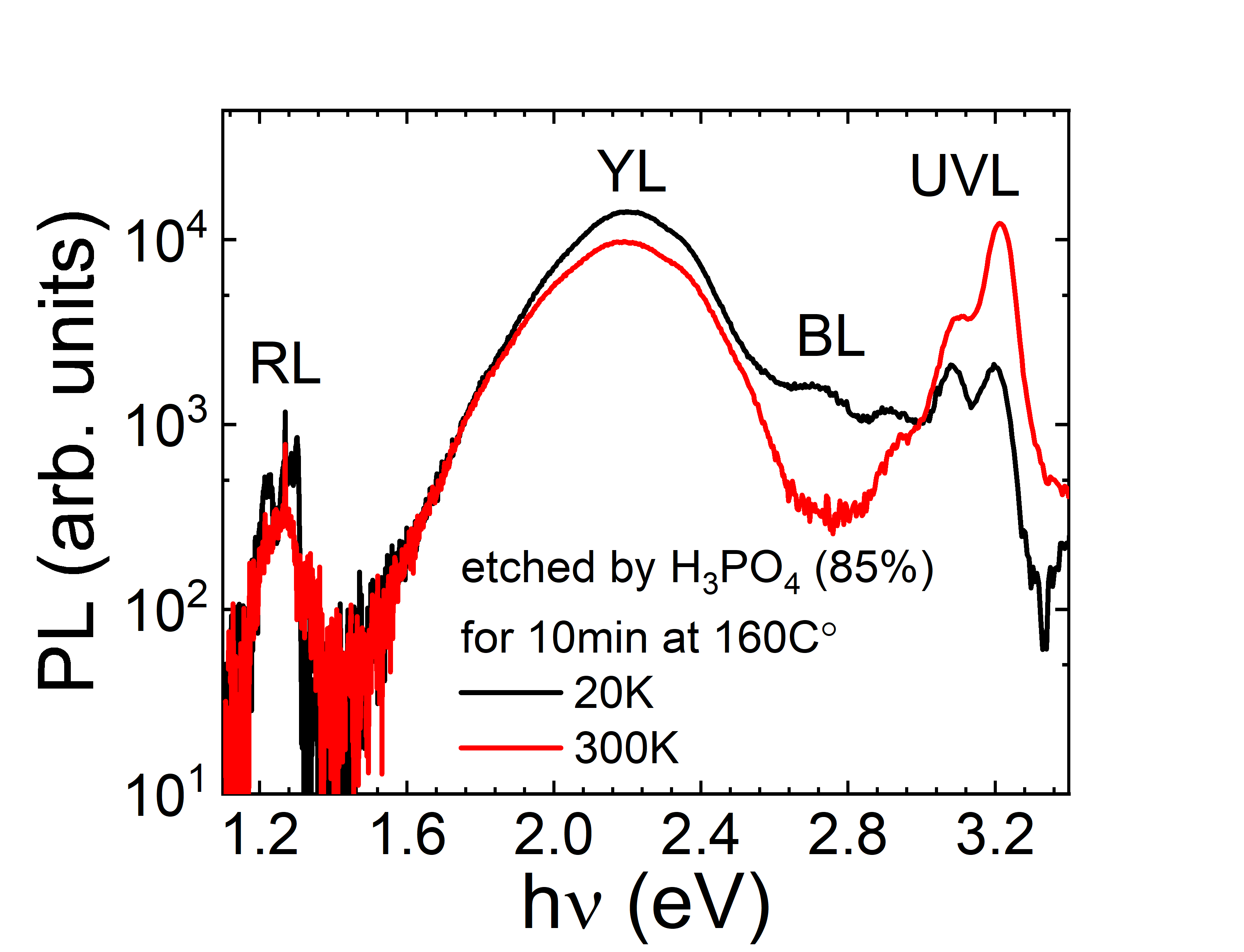
Measurements of electrical and optical properties of chemically etched MOCVD GaN sensors were carried out in the 20-300 K temperature range. The comparative analysis of variations of these characteristics in chemically etched MOCVD GaN will be presented and discussed.