
The search for new materials and the formation of radiation-tolerant sensors devoted for the space industry, the medical diagnostics instruments and the high-energy physics applications is necessary. Binary direct-gap compounds such as gallium nitride (GaN) are effective in producing dual-response (i.e., capable of detecting electrical and optical signals) devices [1]. But due to imperfect MOCVD growing technologies, the formation of various technological defects, which are usually inhomogeneously distributed throughout the crystal wafer [2], is inevitable. These defects determine the optical and electrical characteristics of devices. Therefore, it is important to investigate the distribution of defect species within the MOCVD grown GaN wafer area in order to improve the growth regimes as well as to identify the areas of best quality. Light extraction efficiency (LEE) is another parameter which should be enhanced for efficient device operation. This can be achieved by modifying the surface of the material by using the chemical (wet) etching method [3]. It has been shown that the chemical etching procedures significantly modify the structure of dislocations and their occupied areas and might be the reason of the increase of intensity of scintillation signals in MOCVD GaN based sensors [4].
The aim of this work was the modification of MOCVD grown GaN surfaces by potassium hydroxide (KOH) and phosphoric acid (H\(_3\)PO\(_4\)) and comparative analysis of variations of optical characteristics in respect to etching regimes. The research methodologies like time-integrated photoluminescence (TI-PL), microwave-probed photoconductivity (MW-PC) transient techniques were applied for the investigation. While surface control was realized by optical microscopy imaging.
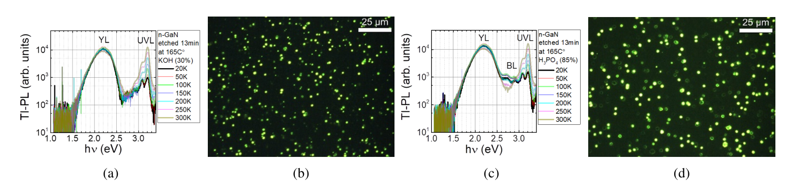
It was deduced by the analysis of PL spectra that the defect distribution in the MOCVD GaN wafer is inhomogeneous, with more carbon and oxygen impurities accumulating at the edges of wafer. It was shown that carrier surface recombination lifetime can be increased by modifying the MOCVD GaN surface using chemical etching. The dislocations act as centers of attraction for point defects, resulting variations in bulk carrier lifetime. The blue luminescence band was observed in H\(_3\)PO\(_4\) etched layers, however this band was absent in KOH modified MOCVD GaN. The variations of intensity of PL bands might be related to modification of space charge region, surrounding the dislocation cores and acting as non-radiative recombination centers. The variations of PL and MW-PC characteristics in chemically etched MOCVD GaN will be presented and discussed.