Today material processing by ultrashort pulses in UV spectral domain allows us to achieve high precision and efficiency. However, in large-area surface patterning optical lithographic techniques [1] are still being used despite having limited selection of usable materials and requiring multiple processing steps, facilities and machines. Therefore, there is a demand for alternative methods such as fs-UV interference processing. This method can produce large areas of periodically arranged structures with a period close to the wavelength of the used fs-pulses. This ensures accurate and fast surface patterning without requiring additional preparation or post-processing.
Fs-UV interference method has a wide range of potential applications in photonics, nanotechnology, or biomedicine. Specifically, it can be utilized to produce functional surfaces that exhibit antireflective [2], antibacterial [3], or hydrophobic [4] properties.
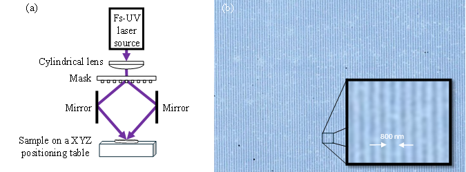
In this presentation, we present our results for two-beam interference patterning using the third (343 nm) harmonic of an amplified Yb:KGW laser system, providing pulse durations of 240 fs. To achieve interference on the sample, a prototype machining head (Talbot interferometer) was constructed (Fig. 1a). This setup has many drawbacks when used with ultrashort pulses [5], thus a Kostenbauder matrix formalism [6] was employed to calculate optimal parameters for the alignment of the pulses. Consequently, homogeneous gratings with nanoscale feature sizes were fabricated on a silicon surface with periods of \(\Lambda = 800\) nm (Fig. 1b). In addition, etching the gratings in a 1% KOH solution resulted in a 10-fold increase in structure height.
In summary, our study showcases the direct processing of centimeter-scale areas through an fs-UV interference method. The Talbot approach not only ensures ease of alignment and precise period control but also offers the advantage of having a compact configuration. Importantly, material removal can be controlled with nanoscale precision.