Silicon material is widely used in semiconductor electronic devices, including irradiation detectors. Its demand is increased with grand applications for large facilities like CERN and many scientists are involved in the research to make Silicon detectors more irradiation resistant by exploiting defect engineering. To make it efficient, the research focuses on techniques like CV, IV, DLTS, TSC, photo absorption and more [1-4], capable to identify the impurities and their impact on the material parameters required for the device performance.
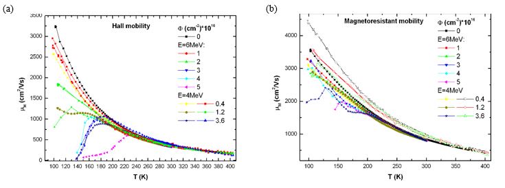
One of the popular techniques is charge carrier transport investigation exploiting Hall and magnetoresistance (MR) effects simultaneously. It is widely used to investigate electrical properties of semiconductors, including n-type Si, but much less information is available for boron doped p-type irradiated Si, where interstitial type defects are essential. So, this work is dedicated to applying Hall and MR effects to evaluate charge carrier transport peculiarities in p-type boron doped Si irradiated with fast electrons.