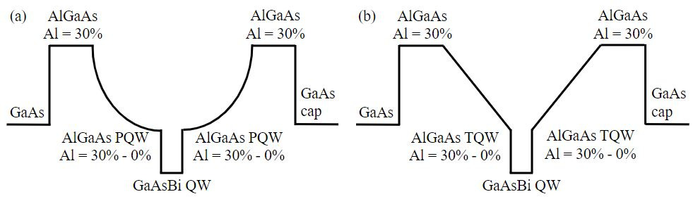
There is a high focus on the task to find a novel light-emitting material, which would serve a purpose of active media in light sources of near-infrared (NIR) range, but would also own superior properties than right now used alloys. One of the potential materials could be GaAsBi. By introducing bismuth atoms into GaAs lattice the bandgap of the alloy is rapidly reduced. Moreover, some unique properties belong to bismides, like large spin-orbit splitting energy and bandgap, less sensitive to temperature. There are already some examples of optoelectronic devices such as light-emitting diodes [1], which work based on GaAsBi. However, the lack of high crystal quality in GaAsBi is reducing the photoluminescence (PL) intensity. Thus, various designs of GaAsBi quantum structures are investigated towards optimization of its optical properties.
Our group [2] already demonstrated GaAsBi quantum wells (QWs) with parabolically graded barriers. Remarkably, a substantial enhancement in PL intensity at room temperature was observed in these structures, exhibiting approximately 50 times greater values than that of rectangular QWs. Moreover, it should be noted that the improved PL intensity was consistently reproducible across various growth conditions in parabolic quantum wells (PQWs). Also, in literature [3] one more design could be found - triangular quantum well (TQW), and its influence on PL was also investigated.
In this work a comparison study between PQW (Fig. 1. (a)) and TQW (Fig. 1. (b)) designs will be done with a goal to look into how barrier design determines carrier trapping and are there any other mechanisms responsible for enhanced PL intensity. Both investigated structures contain single rectangular GaAsBi QW embedded in parabolic or triangular AlGaAs QW. PL and photoluminescence excitation (PLE) techniques along with theoretical calculations will be used to evaluate different barrier design influence on carrier trapping and quality of GaAsBi QW.