
Nitride based laser diodes (LDs) which cover the emission wavelengths from ultraviolet to the green region recently become a subject of intensive studies. The emission wavelength can be engineered by changing the indium composition in the quantum wells - one can shift the wavelength from ultra-violet up to green from quantum wells [1]. For a successful operation of LDs not only perfect structural quality of grown layers is crucial but also the reduction of the optical losses in the laser structure is of the great importance.
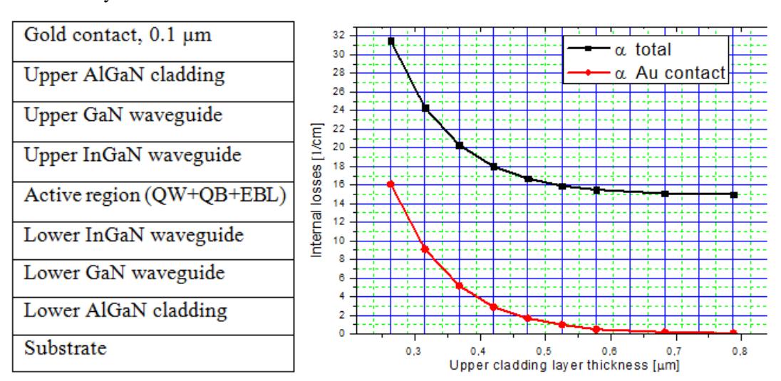
In this work we study a new design for waveguide (WG) and cladding layers (CL) for nitride based true-blue LDs operating at 450-460 nm to reduce optical losses. We calculate the influence of composition and thickness of WG and CL on the confinement factor and internal losses of a LDs (for LDs details see Fig. 1a). A one-dimensional method developed by M. J. Bergmann and H. C. Casey Jr. [2] is used for numerical determination of the transverse electric field distribution. Parameters for calculations were taken from Ref [3]. In Fig. 1b we demonstrate how the thickness of upper cladding layer affects the internal losses. For too thin claddings the mode reaches the highly absorptive upper gold contact which causes unnecessary losses.
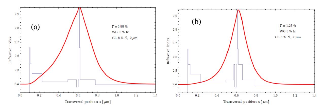
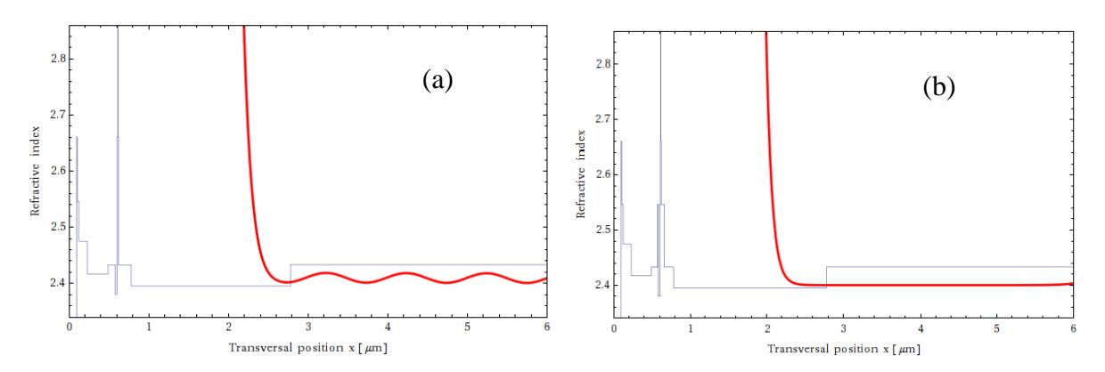
By changing in the composition of waveguide we can significantly modify the operating parameters of a LD. Fig. 2 shows a comparison between two waveguide designs: a) 180 nm GaN waveguide, b) 180 nm GaN with internal 90 nm InGaN high refractive index waveguide. The second design not only gives a higher confinement factor but also lowers the internal losses caused by magnesium doped cladding and gold contact. Fig. 3 shows the magnification of optical intensity from Fig. 2. In case of the waveguide without indium the mode leaks to the substrate which negatively affects the far-field pattern [4]. The design with an internal InGaN waveguide eliminates this phenomenon.
In conclussion, we demonstrated that proper design of the waveguides and claddings reduces the optical losses in the contact layer and the substrate. We will compare one dimensional model prediction with more general two-dimensional method developed by U. Schwarz et al. [5].