InGaN is a defect-rich material with typical dislocation densities of more than 108 cm-2 [1]. Despite this fact InGaN materials are efficient light emitters and currently are used in fabrication of various optoelectronic devices, such as green, blue and white light-emitting diodes and lasers. Some of InGaN luminescence peculiarities are described by carrier localization model. During the growth of InGaN epitaxial layers indium tends to form higher concentration areas, which act like quantum wells [2]. Free carriers prefer to localize in those areas and more likely recombine radiatively. Since most of the photoluminescence (PL) comes from indium-rich areas, spatial distribution of the PL in an InGaN are non uniform and PL from high intensity region tends to have longer wavelength of the spectrum peak than from the low intensity region. Besides the band edge PL, InGaN emits longer wavelength radiation caused by the energetic levels of defects. The defect-related emission broadens the PL spectrum and lowers the band edge luminescence causing the reduction in the efficiency of InGaN-based devices.
In this work, investigation of influence of laser annealing on InGaN epitaxial layers was performed. InGaN epitaxial layer grown by MOCVD technique over sapphire substrate was annealed with various laser intensities (ranges from 4.2 MW/cm2 to 25 MW/cm2) in 6 different locations. High intensity laser annealing effect to the surface was visible even to the naked eye. The surface relief was investigated using atomic force microscopy technique. Laser annealing causes the formation of bumps with bigger radius, but smaller height.
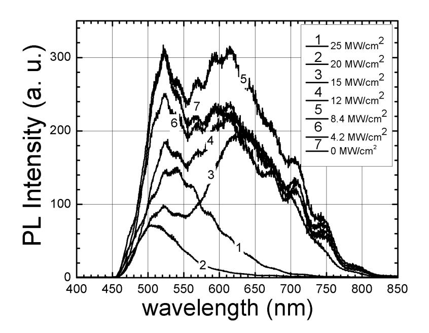
The PL spatial distribution was obtained from all the annealed areas and the initial area for comparison using laser scanning confocal microscopy technique. Spatial distribution of the PL intensity from all areas was strongly inhomogeneous. Spatially integrated spectra illustrated in Fig. 1. The PL spectrum from the initial area has both band edge and defect-related band with equal intensity. Laser annealing has considerable influence on the shape of the PL spectrum at higher intensities than 12 MW/cm2. At ≥20 MW/cm2 annealing intensities, the defect-related band disappears, but the intensity of the band edge PL decreases.