
Ion implantation is a technological procedure widely used in semiconductor device fabrication. Carrier lifetime is one of the most sensitive parameters to defects in semiconductor materials. Therefore defect introduction by high energy particle irradiation is an effective technological tool for manipulation of semiconductor device characteristics. Consequently, in situ control of defect introduction and their evolution during implantation of different ions is important for development of the radiation technologies in micro- and nano-electronics [1]. Contactless transient technique, based on analysis of the microwave probed photoconductivity dynamics, has been employed to monitor the evolution of defects in silicon during proton irradiation. A sketch of the measurement setup, containing an irradiation chamber installed within particle accelerator Tandetron 4110A and an instrument for carrier lifetime in situ control, is illustrated in Figure 1.
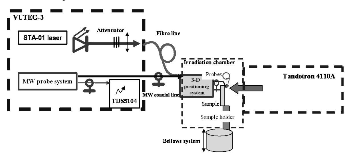
In this work, carrier lifetime variations ascribed to 1.5 MeV proton implantation induced radiation defects, acting as fast carrier traps, are analyzed. Changes of the surface and bulk recombination components revealed within photoconductivity transients recorded in 300 μm thick SiO2 passivated Si wafers under various particle fluences and exposure times will be discussed.