
Heterojunction based on tin dioxide films and silicon, are interesting structures for building gas sensors, that's why the investigation of its electro-physical characteristics took place.
The investigated experimental structures were made by spray pyrolysis from solution on p-type silicon plate. Were received samples with tin dioxide film thickness 4, 7, 10, 15, 20 and 30 nm. Current - voltage characteristics (C-V) were measured in voltage range -1,5÷1,5 V (Fig.1).
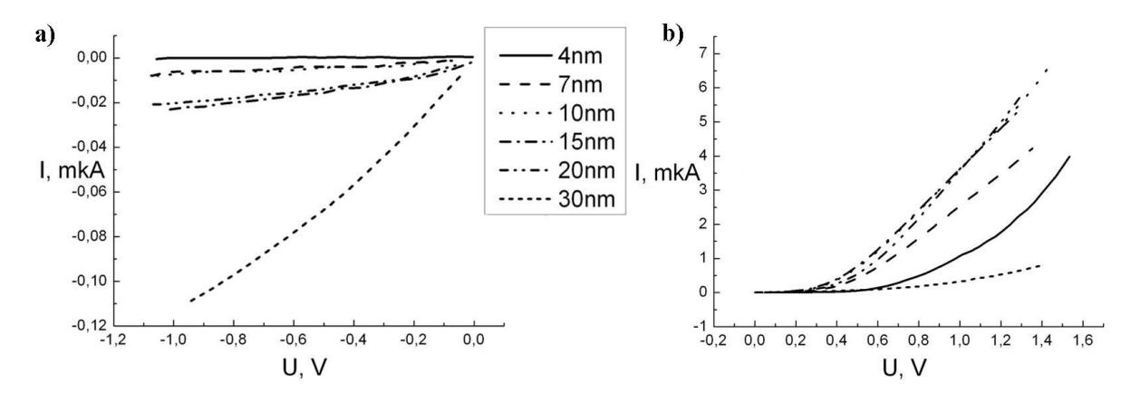
C-V analysis carried out in the approximation of over-barrier current transport mechanism. For semiconductors charge transfer can be described by thermionic over-barrier emission for majority carriers.
Barrier height dependence on SnO2 film thickness is shown on Fig.2. The barrier height decreases with increases of a thickness of a film from 4 to 15 nm. After that it gets out on saturation and does not change at the subsequent increase of a film thickness to 30 nm.
As atomic-force microscopy studies have shown tin dioxide films have discontinuous structure. When they are nanoscale they may grow with mechanism of Stranskoho - Krastanova. The number and size of islands varies with the film thickness by qualitatively law. With increasing of film thickness islets dimensions increases, until they begin to merge with each other. The mean surface roughness (as follows from the results of atomic force microscopy) decreases until becoming constant value on film thickness at about 20 nm.
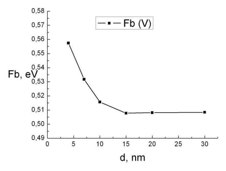
Accordingly to the reduction of mean surface roughness, adsorption-active surface area of metal dioxide film decreases. This reduces the number of traps on the surface of SnO2, which arise as a result of oxygen adsorption on oxygen vacancies. Presumably, this dependence of film morphology explains the dependence of heterojunction barrier height on the thickness of metal dioxide film.