
Despite the significant advances achieved in DPSS lasers with thin disks and crystal rods lasing medium architecture during last decade, the considerable problems are encountered in practical employment of such lasers in industrial micromachining processes. Harsh conditions, which are often met in industrial environments, strongly affect reliability and durability of DPSS lasers. Also, in order to achieve relatively high pulse energy, lasing medium cooling issues arise to be dealt with [1]. Advantages of DPSS lasers such as availability of higher harmonics generation are difficult to apply due to costly harmonics generators and thus expensive optical components required. Usually higher throughputs are more important for the industrial processes than the best possible fabrication quality gained. Obviously, as new solutions for rapid industrial micromachining are necessary, diode - pumped fiber lasers could be a possible choice to overcome the problems mentioned above [2, 3].
Silicon being one of the most significant elements used in nowadays industry, was chosen to be as a sample material for micromachining using high brightness Yb doped fiber laser based on MOPA architecture ($E_{max} = 1 \text{ mJ}$, $\lambda = 1070 \text{ nm}$, $\tau_{pulse} = 120 \text{ ns}$). The main objective of our experiments was to define the set of micromachining parameters for high - speed silicon wafers cutting. Both crystalline and poly – crystalline silicon wafers were used for cutting process development. X–Y positioning system with accuracy of 1 μm and $v_{max} = 500 \text{ mm/s}$ was employed for sample scanning.
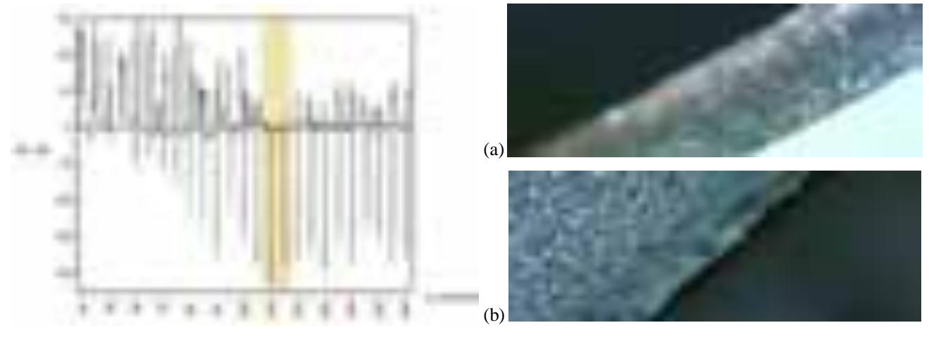
Silicon ablation rate dependence on laser beam scanning speed was evaluated. In Fig. 1 the profiles (measured using stylus profiler Dektak 150) of kerfs formed in silicon wafers using different laser beam scanning speeds are presented. The optimal scanning speed was estimated to be 110 mm/s which correspond to 85 % laser pulse overlap. Average cutting speeds of 2.5 mm/s (for crystalline silicon) and 3.3 mm/s (for poly – crystalline silicon) were achieved (wafers' thickness 450 μm). The quality of cutting edges can be seen in Fig. 2. Heat affected zones and micro cracks penetration was observed in the width less than 20 μm for crystalline and less than 30 μm for poly-crystalline silicon wafers.
Our experiments revealed that silicon wafers laser cutting process using high power nanosecond fiber laser could be considered as a key technology for semiconductors electronics and solar energy industries and should be developed further. Optimal set of parameters for both crystalline and poly-crystalline silicon wafers micro-cutting was defined. The throughput of the process is high enough while keeping required quality of structures micro machined. Relatively low price of MOPA architecture based laser systems leads to cost effective process for R&D activities as well as mass production.