
Structural and electronic properties of the GaBixAs1-x ternary alloys as well their growth technology became important in recent years because of promising applications in ultrafast electronics for the near infrared region of 1 – 1.5 µm [1,2]. The Bi-induced atomic disorder results in a strong reduction in the band gap Eg for a relatively small alloy concentration (62 meV per 1% of Bi) [1-3] and strongly influences carrier recombination features [4-6]. In this work, I investigated nonequilibrium carrier recombination and transport characteristics of GaBiAs layers grown under different conditions, and studied the suitability of GaBiAs compounds for semiconductor saturable absorber mirrors (SESAM).
These studies were performed using optical pump-probe and transient gratings (TG) experimental techniques. In the studies I used picosecond pump-probe setup designed to measure light-induced refractive index ($\Delta n$) and optical transmittance change ($\Delta T$) dynamics over a wide excitation energy and delay range. Nonequilibrium carrier lifetime was determined from the differential transmittance relaxation rate $\Delta T/T$ whereas diffusion coefficient and carrier lifetime values at lower excitation densities were determined from the diffraction signal kinetics. Differential transmittance measurements were also carried out for characterization of saturable absorbers.
In this study, d=1.2 – 1.5 µm thick GaBiAs layers with different molar concentrations of Bi have been grown by molecular beam epitaxy (MBE) on GaAs substrates. Energy band gap Eg of the GaBiAs alloys, determined from the absorption spectra, ranged from 1.04 eV to 1.38 eV and provided the Bi content in the samples. Optical measurements revealed that distribution of bismuth atoms is likely non-homogeneous resulting in diffusive wash-out of absorption edge (within 40 – 150 meV range) and pronounced carrier localization effects, in addition to the valance band shift.
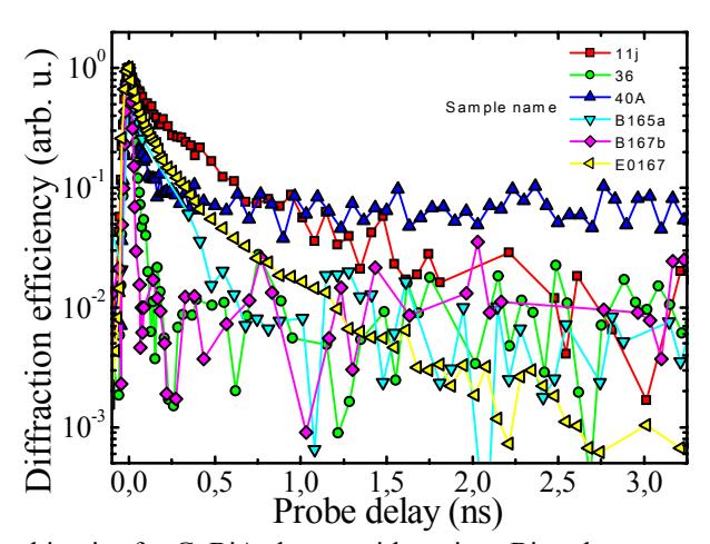
TG measurements showed that at least two types of recombination processes take place in GaBiAs layers. Decay transients of TG signal are nonexponential – in most of the samples I observed rapid initial and slower later components (Fig. 1). The initial component decay time varied from 27 to 1110 ps, while the slow component decay time was as long as 300 - 800 ns. TG measurements with different grating periods also showed that the diffusion coefficient of the carrier associated with slow component was immeasurably small (<0.1 cm2/s) while the initial component diffusion coefficient was much higher (0.94 cm2/s). From the later data, it was concluded that the initial component of TG kinetics reflects recombination of free carriers, while the slow part – recombination from the localized carrier states.
The samples were characterized as a SESAM active material by measuring the following parameters: response time (<25 ps – 1.2 ns), saturation energy fluence (55 µJ/cm2 – 1.6 mJ/cm2) and modulation depth (10% – 200%) at 1064 nm. These parameters are comparable with the parameters of saturable absorbers on the market, so GaBiAs could be used as a full-fledged alternative to other semiconductors, for example InGaAs.