
There is an increased interest in terahertz technologies for imaging and spectral analysis in security, medical and inspection applications. That is why research of new terahertz detector types for almost a decade has been one of the "hottest" trends in solid state physics [1]. By means of new opportunities given by modern physics and technologies, several detector types were proposed. Unfortunately their operation is often bond to low temperatures. Alternative way of detecting THz frequencies is based on plasma wave excitation in ballistic field effect transistors (FETs) and for the first time was proposed by M. Dyakonov and M. Shur [2, 3]. It appears that such detectors can operate at room temperatures. Theory additionally suggested few important conclusions: 1) plasma wave frequency can be tuned by the gate voltage, 2) depending on external factors, detectors can work as resonant or non-resonant, 3) detector operation has no temperature restrictions [1].
Detector theory also predicts possible improvement of signal detection by current biasing transistor channel. However, experimental studies present, that in these conditions, device noise increases drastically, what can lead to the lower signal to noise ratios than in not biased devices. In order to clarify this matter, we present low frequency noise and detection characteristics study of silicon based CMOS detectors in both biased and not biased regimes.
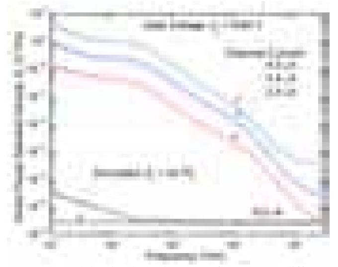
Fig 1. represents noise power spectral density dependence on frequency while transistors gate voltage is set to 0,64 V and it operates at different bias conditions. One can notice, that at zero bias the only noise source at middle and high frequencies is channel thermal noise (it perfectly matches its theoretical value given by 4kTR, where R is channel differential resistance) but at currents higher than 0 μA, it is strongly exceeded by 1/f and generation-recombination (GR) type fluctuations. The reason of such strong excessive noise is random carrier generation-recombination processes through impurities and GR centers dislocated in both transistors channel and oxide layer. Moreover, by driving detectors close to the saturation currents, differential resistance increasement (what leads to channel thermal noise increasement) should be taken into account as well.
All in all, although silicon CMOS technology based detectors can experience significant signal increase with applied current, this enhancement is strongly threatened by excessive 1/f and GR type fluctuations and thermal channel noise increasement with applied source to drain voltage.