
III-V semiconductor compounds offer a large amount of advantages, especially in optical applications. Many of them are direct band gap materials, and therefore emission and absorption of photons are favored compared to indirect bang gap semiconductors. Properties like band gap or carrier mobility can easily be changed by varying the proportions of the materials used in binary, ternary or quaternary compounds. This makes it possible to develop complex heterostructure solar cells, light emitting diodes and other useful devices.
Some combinations of III-V materials cannot be grown in planar structures, as the lattice constants differ too much and defect would be formed at the interface. Due to this properties of the fabricated device are degraded. Growing the structures in a nanowire form avoids this problem in releasing strain by radial relaxation. This results in defect free semiconductor heterostructures and even better, allows growing them on top of silicon with intention of easy integration with already existing silicon technology.
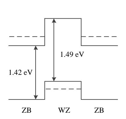
Indium phosphide (InP) nanowires were one of the investigated objects. Usually, undoped InP nanowires show an equal share of zincblende (ZB) and wurtzite (WZ) crystal structure [1]. The amount of WZ can be increased by n-doping with sulfur during the growth process. As the WZ crystal structure of InP does not exist in bulk material, it is not fully investigated, but some interesting properties are already known, for example, the existence of a second conduction band 0.24 eV above the first one [2]. The mixture of ZB and WZ InP forms a type 2 alignment. Figure 1 indicates the spatial separation between the electrons and holes in it. The ZB segments act as traps for electrons and therefore the conductivity is determined by the longest ZB segment [3].
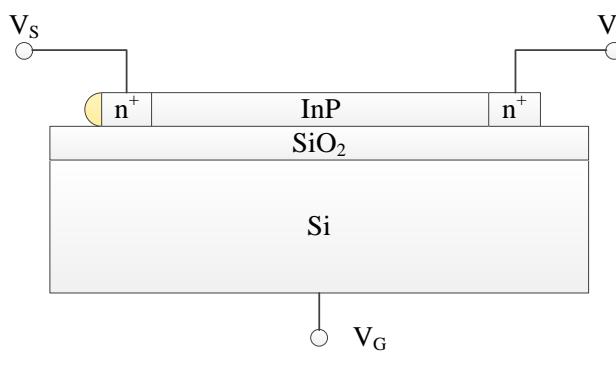
We used a Fourier transform spectrometer to investigate single InP nanowires with different doping levels (fig. 2). Spectral photocurrent measurements did not show a blue shift for highly n-doped nanowires which would correspond to state filling in the conduction band. Furthermore, electro-optical properties of GaSb/InAsSb/InAs nanowire based infrared photodetectors were investigated.