
Gallium nitride (GaN) is leading material in bright light-emitting diodes since the 1990s. Its wide band gap of 3.4 eV affords special properties for applications in optoelectronic, high-power and high-frequency devices. Control over defects in the material growth is the main task to ensure quality of future products. One of the most serious problem in development of III-N based devices is lack of suitable substrate material on which lattice-matched layers can be grown. The collection of extended structural discontinuities in the lattice, such as interfaces, dislocations and stacking faults, is referred to as the microstructure of the material. The microstructure is sensitive to steps involved in crystal growth, such as the substance used for epitaxy, the growth method itself, and variations in chemical composition during growth. By far the most useful substrate to date is sapphire. This is surprising given the large differences in thermal expansion and in lattice parameter between sapphire and the nitrides. However, epitaxy of nitrides on sapphire has produced the best device performances [1]. Notwithstanding, the nitride materials, grown on sapphire contain a large density of threading dislocations. It is well established that threading dislocations are degrading the performance and the operating lifetime of optoelectronic devices [2].
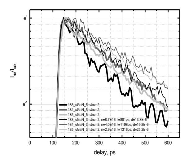
Institute of Applied Research, Vilnius University, works on GaN growth using metal organic chemical vapor deposition (MOCVD) and characterization of grown layers. Our interest in growth of GaN concerns evolution of defects, when higher thickness of layer is reached (up to ~25.2 μm). Structural quality of a set of samples with sequential increase in thickness was inspected first using optical and electron microscopy means. Using Hall measurement technique the mobility and equilibrium carrier concentration in the samples were defined. Due to these results, a decrease of dislocation density with increasing thickness of samples was observed. There was not enough to have these results to ensure correct characterization of GaN layers because of some indeterminacy. To investigate carrier dynamic light-induced transient grating (LITG) technique was applied (Fig. 1). Results from this method have supplemented previous hypothesis, however, raised some new questions which we intend to resolve using alternative techniques: XRD (measurements to determine lattice plane imperfections in direct way), electron microscopy (SEM, TEM).
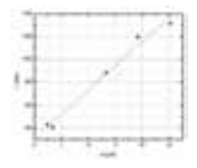
The obtained dependence between thickness of the layer and carrier lifetime could be explained by the existence of less frequent dislocations due to improved base structure (grown in several stages) (Fig. 2). According to our measurements (around 30 samples), it is possible to determine optimal growth conditions (temperature, steam of NH3, duration regimes, etching time and temperature).