
The operational characteristics of semiconductor power devices strongly depend on junction, formed by technological procedures, profiles and depths. Junctions are commonly formed by thermal diffusion procedures when dopant atoms are introduced. However, together with the dopants, undesirable impurities can be introduced as well, which affect the device functional parameters. On the other hand, certain impurity atoms (gold, platinum) can be intentionally introduced or ions can be expediently implanted to create the enhanced recombination layers of various profiles within power device structures and to handle the switching rates of power devices. Thus, these modifications of material should be precisely controlled to predict the operational characteristics of devices.
Various techniques are employed in profiling of the chemical structure of materials, such as scanning spreading resistance microscopy (SSRM), scanning capacitance microscopy (SCM) [1]. However, these techniques do not provide information about undesirable impurities or defects introduced during implantation.
In this work a technique for barrier evaluation by linearly increasing voltage (BELIV) is presented based on measurements of current transients at reverse and forward pulsed bias [2]. This barrier control technique is combined with a step-positioning of the needle-tip probe, located on the cross-sectional boundary of a parallel-plate layered structure [3]. The spreading current pulsed measurements are performed by scanning a boundary of the structure using the needle-tip electrode. The other contact is connected to the parallel plate electrode at sample surface. When a needle probe is positioned at the same layer as the plate electrode, the measured transient then repeats the linearly increasing voltage pulse shape and its amplitude depends on the layer resistance. The barrier charging and charge extraction currents are measured when the probe is positioned at the other layer of the junction. Spreading resistance, barrier capacitance and parameters of deep traps can be evaluated when analyzing the shape, the amplitude and duration of measured current transient. Profiles of the current amplitudes and transients duration, which correspond to the profile of dopants density, measured in pin diode structure are presented in Fig. 1.
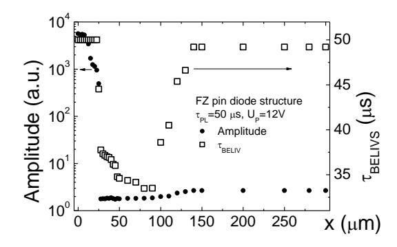
Variations of barrier capacitance and spreading resistance parameters measured in power pin diode and thyristor structures by employing the BELIV technique will be discussed in this presentation.