
Doped silicon is a promising candidate for quantum computing due to its scalability, long spin coherence time, and the amazing progress in Si technology. The precise control of the dopant position is necessary for the experimental realization of such a working qubit. For fundamental physics as well as for applications it is interesting to develop models for a better understanding of the physics of single dopants localized near an interface taking into account the complete electrostatics of the problem, i.e., the image charges and a gate of finite size. For the case of a semiconductor/metal interface the energy spectrum was recently investigated in [1] using the finite element technique and in [2-5] the ground state energy of a donor localized in Si near an interface with an insulating layer (semiconductor/dielectric system) was calculated using a variational approach. In many of those calculations it was suggested a metallic gate is of infinite size. However one needs to use more realistic models to study this problem. This work suggests that the gate has nanoscale dimensions which is expected for future devices.
To calculate the electronic spectrum and electrons wave function $F(\vec{r})$ an eigenvalue problem for the following equation (written in dimensionless form) should be solved:
$$ \left\{ -\nabla^{2} - \frac{2}{r_{D}} + V_{imp} + V_{simp} - e\varphi_{0}g(\vec{r}) \right\} F(\vec{r}) = EF(\vec{r}), \qquad \tag{1} $$where $V_{simp}$ describes the interaction between electron and its image, $V_{imp}$ is the interaction between electron and donor image, $\varphi_0 g(\vec{r})$ is the potential landscape in the semiconductor due to the gate, $r_D$ denotes the distance between electron and donor. All distances are scaled to units of gates diameter (d) and the energy E is given in effective units of $\frac{Ry^*}{\delta^2}$, where
$\delta = \frac{d}{a^*}$. $V_{simp}$ and $V_{imp}$ can be represented in an analytical form. The value of potential $\varphi_0g(\vec{r})$ was calculated using finite element method with approximation by linear finite elements on a triangular mesh. The gate voltage is cylindrically symmetric, so cylindrical coordinates were used. The equation is posed in a bounded domain $\Omega=[0,L_p] \times [0,L_z]$ chosen for an approximation of the semi-infinite region $[0, +\infty] \times [0, +\infty]$. These calculation were carried out using MATLAB. The problem (1) itself was solved using finite element method.
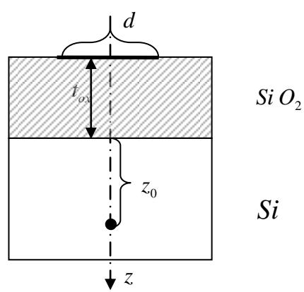
Using the suggested approach, we have studied the P donor wave function perturbed by an electric field and the Si host geometry, effects of varying several experimental parameters: the gate voltage, donor depth and the gate diameter were examined in order to find conditions of electron shuttling between donor position and surface. The presented results highlight not only the significance of the gate potential in affecting the donor electron wave function, but also the position of the qubits in the device. The proximity of the qubit to the gate is also important in determining the degree to which the electron exchange interaction can be enhanced by the applied voltage.