Nitride semiconductors have been widely investigated during the last two decades due to their exceptional material properties. The band gap of ternary InGaN compound can be varied from 0.7 eV (InN) to 3.4 eV (GaN). Thus, InGaN enables fabrication of red, green and blue light emitting diodes (LEDs) using single ternary alloy. InGaN-based blue LEDs are already commercially available. However, realization of efficient InGaN-based LEDs emitting at longer wavelengths is still a major challenge, mainly due to high defect density of the active layer.
The emission efficiency in InGaN active layer can be enhanced by coupling the optical transitions in InGaN multiple quantum wells (MQWs) with localized surface plasmons (LSPs) in silver nanoparticles (NPs). Since the density of states of LSP mode is large, the QW-LSP coupling rate is fast and it creates a new path for radiative carrier recombination. On the other hand, QW-LSP coupling might also improve the light extraction efficiency.
In this work, the enhancement of InGaN MQW photoluminescence (PL) by LSPs in silver NPs is investigated. InGaN/GaN MQW structures were grown by metal-organic chemical vapor deposition (MOCVD) on sapphire substrates at the Institute of Applied Research. Silver NPs were fabricated by thermal annealing of thin silver layers deposited on the MQW structures. Silver layers of 5 nm, 8 nm and 12 nm were annealed at two different temperatures (500°C and 300°C).
The samples were investigated using WITec Alpha300 microscope system working in confocal spectroscopy and atomic force microscopy (AFM) modes. The surface configuration and dimensions of fabricated nanoparticles were characterized using AFM, while the spatial distributions of photoluminescence parameters were measured using confocal microscopy technique. PL was excited using a CW laser diode ALPHALAS emitting at 405 nm. Absorption spectra of each sample were measured using Perkin-Elmer Lambda 950 spectrometer and enabled to determine the wavelength of LSP resonance.
The study of surface morphology showed that annealing at a higher temperature is more favorable for the formation of larger and better separated NPs. It was found that annealing of the thickest silver layers (12 nm) at both temperatures resulted in formation of large NPs (>100 nm in diameter), while smaller NPs (<75 nm in diameter) were formed from 5 nm and 8 nm thick layers.
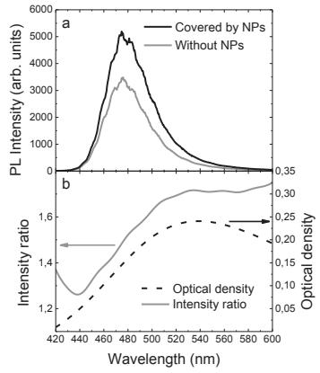
The measured optical absorption spectra showed that the resonance in larger NPs is better pronounced and occurs at longer wavelength. Moreover, stacked nanostructures exhibit broadening of the absorption bands.
Confocal PL imaging measurements were performed on the surface of the sample with and without silver NPs. The measurements revealed that the amplification of PL intensity is observed only in samples with the largest NPs. The increase of PL intensity (by ~53%) is larger in the sample with the thickest silver layer (12 nm) annealed at lower temperature (300°C) (see Fig. 1), due the better match between the surface plasmon resonance wavelength and the PL emission.