
CdTe is a compound semiconductor involving a large concentration of defects produced during growth and material processing. A large number of defects have been detected using a number of techniques: the deep-level transient spectroscopy(DLTS), photo-induces current transient spectroscopy(PICTS)[1]. But, for highly resistive materials DLTS is not useful. Also, PICTS can't give information about the sign of Hall voltage.
CdTe has long been know as an interesting semiconductor with applications such as gamma ray detection and solar cell fabrication. Many of the physical properties of CdTe are controlled to some extent by the relative position of the energy levels within the forbidden gap associated either native defects or impurities. Only by understanding the nature and origin of the defects, can their concentration be controlled[2].
In this presentation we extend our previous studies of deep levels in CdTe done by photo-conductivity and Pockels effect measurements [3]. In view of the fact that these methods bestow only indirect information on the character of principal deep levels, we study the transport of photoexcited charge in the magnetic field where the sign of Hall voltage gives us an explicit evidence on the level [4].
The principle of the research is apparent in attached figure(fig.1). In case of trap level localized in the upper part of the forbidden gap the dominant optical transitions will excite electrons at the energy ET1 - EV from the valence band creating positive holes there and inducing positive sign of the Hall voltage. Oppositely, the level at the bottom part of the gap will induce the negative Hall voltage after the excitation at the energy EC - ET2.
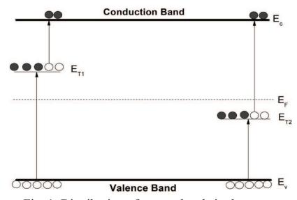
Spectral measurements of the photo-Hall effect were used to determine energy levels responsible for polarization and to find the optimal wavelength for optical depolarization of the detectors[3].