Indium gallium nitride (InGaN) has been the subject of extensive research, because of their wide application in optoelectronics. InGaN can cover light spectrum from near-infrared to ultraviolet range, depending on In and Ga concentration ratio in alloy. The growth of high quality InGaN multiple quantum wells (MQW) is a great challenge, because of lattice mismatch between InN and GaN and the different growth temperatures.
The main goal of this work was to optimize MOCVD growth conditions in order to get InGaN MQWs structures with high luminescence efficiency at around 400 nm.
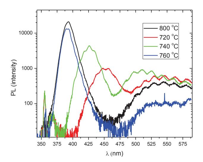
$In_xGa_{x-1}N/GaN$ MQW structures were grown on sapphire C-plane substrates with GaN buffer layer in a vertical flow close-coupled showerhead reactor. We used standard precursors for GaN MOCVD growth – trimethyl gallium, trimethyl indium, ammonia and hydrogen for GaN or nitrogen for InGaN as the carrier gases. The growth was monitored using in situ laser interferometer, determining process steps. The set of samples were grown by using different growth temperatures of the MQWs (720 ÷ 800 °C).
Indium concentration was determined using photo-luminescence and X-Ray diffraction measurements.