In industry of optical coatings silicon dioxide (SiO2) is commonly used as low refractive index material [1, 2]. Reactive magnetron sputtering technique was used for preparing SiO2 thin films. Since pure silicon is insulating material it can only be sputtered using radio frequency (RF) power supply. The main goal was to sputter silicon using direct current (DC) power supply, since plasma created by DC power suply is denser and concetrated closer to target [3]. That lets to avoid plasmas interaction with substrates, increases deopsition rate [4]. For those reasons conducting boron doped silicon target was used.
SiO2 coatings were deposited on fused silica substrates by reactive magnetron sputtering. In basic magnetron sputtering process a target is bombarded by energetic ions generated in glow discharge plasma. The bombardment process causes the removal of target atoms, which then condense on a substrate as a thin film.
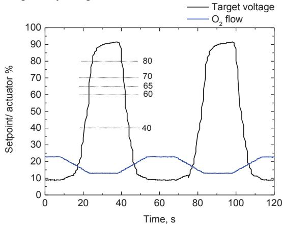
Single layers of SiO2 were deposited using different process parameters such as oxygen flow and target voltage. Fig 1. shows target voltage dependance on oxygen flow. Different setpoint values were chosen for depositing SiO2 layers. Optical properties (refractive index n and extincion coefficient k) were determined from transmitance spectra which was performed in 190-1000 nm wavelength range. Surface roughness of thin films were measured using atomic force micrscope (AFM). All optical and physical properties of SiO2 layers prepared by DC reactive magnetron sputtering were compared to SiO2 layers prepared by RF reactive magnetron sputtering.