
The plasma enhanced chemical vapor deposition of SiO2 was carried out in a vacuum chamber installation YPM 3 3.279.050 with the use of an inductively coupled high-density plasma source operating at 13.56 MHz frequency 240 mm diameter The initial pressure in the chamber is not worse than $3\cdot10^{-3}$ Pa. The operating pressure in the experiments was within the range from 1 to 10 Pa. [1]. The TEOS tank temperature is 21°C. Also the silicon oxide films deposition with different flow ratio of argon and oxygen into the chamber were carried out (Fig. 1).
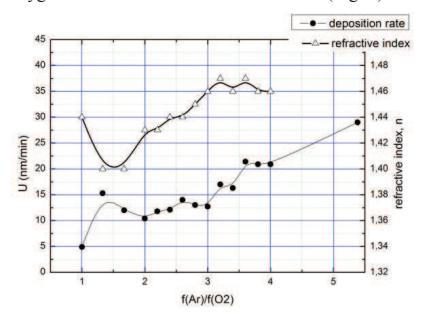
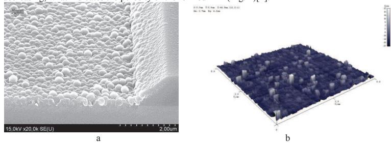
The flow ratio of argon to oxygen flow varied from 1 to 10; besides the argon flow rate was constant and equal to 110 sccm. The pressure in the chamber varied from 2.5 to 5 Pa. We see that the reduction of oxygen in the steam-gas mixture linearly increases the growth rate of the film, with the ratio $f(Ar)/f(O_2)$ more than 4. The refractive index n exceeded 1.52 in the same conditions, simultaneously the transparency of the film was deteriorating. With the flow ratio $3 \le (Ar)/f(O_2) \le 4$ the deposition rate increased, and the refraction index was within $1.46 \le n \le 1.47$, what shows the good quality of the formed film. With the ratio $f(Ar)/f(O_2) \ge 3$, the deposition rate is more complex: it decreases to the ratio of two, then it increases within the ratio of 1.25-1.75 and then decreases again. In this case, the refractive index is constantly decreasing, what indicates the porosity of the formed film (Fig. 2)[2].
The analysis of the experimental results shows that the method of dielectrics deposition in a high-density plasma allows to deposit stoichiometric silicon dioxide films at a substrate temperature of 200 °C, and at the same time stoichiometry can be controlled by varying the reaction components ratio.