
Sapphire Al2O3 wafers are usually used as wafers in manufacturing of light emitting diodes (LEDs). Properties such as high thermal conductivity, transparency in a wide range of wavelengths and crystallographic similarity to GaN makes it the best substrate for epitaxial growth of GaN. Scribing these wafers into small LED chips is essential in the manufacture. Several scribing methods, included laser fabrication, are being analyzed.
One step is the growth of semiconductor materials on the surface of the substrate, during this step there is necessity of the similarity between the structures. The hexagonal structure of GaN demands same or similar structure as well. Despite that it would be ideal to use the same material as the substrate, its' high cost and difficulty of production makes it not applicable. That is why we need alternative substrates and many including based on Si were invented, however neither are as good as made of synthesized sapphire. The deviation between the crystallographic structures is approximately 13%, high transparency gives the possibility to transfer the light through the wafer.
Other step is the scribing of the wafer which leads to thousands of LEDs in the size of few hundred μm and importance of this is not lesser. Industrial applications utilize diamond blade or ablation by nanosecond laser [1]. Their low efficiency led researchers to development of new method – stealth dicing (Fig. 1).
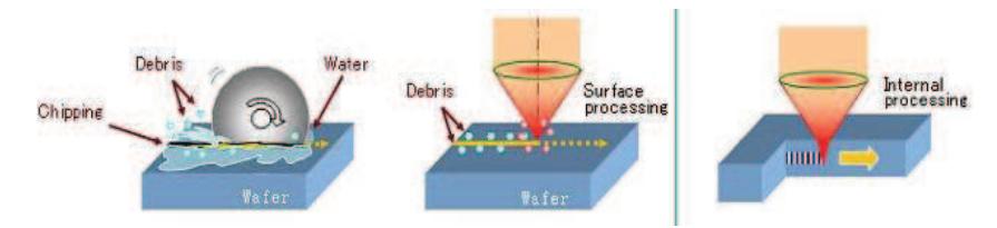
The experiments were carried out by using picosecond laser and simple diamond blade for the comparison. It was proved that the stealth dicing by using picosecond laser is the most effective method, while diamond disc dicing and ablation was not as accurate as crack width was bigger and additional debris occurred.