
Ceramics such as alumina are widely used as substrates or components for electric applications. Due wide range of applications these ceramics need to be manufactured in different shapes and sizes. Laser technologies may give the precision and be efficient enough.
During this experimental work ceramics were diced by using nanosecond laser Baltic HP (Ekspla) irradiation at 532 nm wavelength. Laser beam positioned by galvanometer scanner (ScanLab). The task was to get the highest possible cutting speed so the highest pulse energy of 360 uJ was selected. The method of dicing ceramics is so called scribe & break method as the samples are not scribed through their whole thickness and even though the mechanical breaking is needed it is the most efficient method.
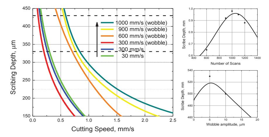
The achieved dicing results point that the wobble option adds only slight but still an increase in the scribing depth. The best wobble parameters where considered to be 1.5 kHz at repetition rate and 5 μm at amplitude. While it is understandable that by increasing scanning speed we widen the distance between pulses, it was proved that to assure a good break we need a distance lesser than the width of a single pulse. As we see in figure, for a sample of 1mm thickness we need a scribe of 330-430 μm and that may be achieved by the scanning speed as high as 1000 mm/s, according to this the obtained cutting speed would vary from 0.6 to 0.85 mm/s, the thinner sample of 0.635 mm thick required only 200-300 μm to break, so the cutting speed was progressively bigger.