
Formation of various nano structures on solar cell surface is becoming one of the most popular ways to improve them. This increased surface roughness allows us to improve some qualities of solar cell such as short circuit current [1].
While forming complicated nano structures on surface of solar cell we have to evaluate some geometrical properties of p-n junction, such as its depth from the surface and its steepness, to make it certain that solar cell is being used optimally. These properties are conveniently measured by Scanning probe microscopy (SPM). Because it allows us easily collect data about nanometric scale objects with p-n junctions in them and there are different types of atomic force microscopy witch could be used depending on our needs [2].
In order to test physical parameters that can be extracted form the measurements of different types of microscopy, GaAs sample was selected as a reference sample. For the measurements we used three different modes of SPM, namely scanning Kelvin probe microscopy (SKPM), electrostatic force microscopy (EFM) and conductive atomic force microscopy (C-AFM). In all cases p and n regions can be identified. However precision of identified regions for different types of microscopy differs.
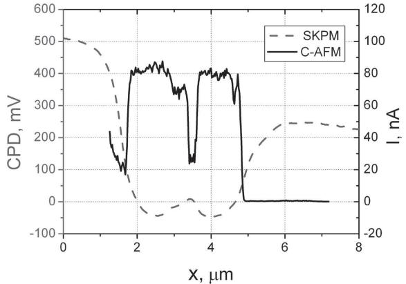
As it can be seen form the Fig.1, contact potential difference (CPD) between sample and microscope's tip measured by SKFM is the least precise due to interaction between sample's surface and cantilever on witch tip is located, this causes some roundness in response signal. This roundness can be avoided by using EFM, as it measures variation of the local electric force gradients above the surface and influence of the cantilever in measured signal can be neglected in most cases. Alternative method, C-AFM measures sample's electrical current at any chosen surface point when external voltage is applied between tip and the sample. The major drawback of this type of microscopy is formation of oxide layer on some materials, which is caused by external voltage applied to the tip of a microscope. This oxide layer limits the repeatability of measurements, because every new measurement adds a new layer of oxide witch weakens the response signal. This effect is a major problem for measurements on Si samples. Also naturally formed SiO2 had a big impact on measurements made with SKPM. We discuss the measurement conditions that can improve evaluation of geometrical properties of p-n junction.