
Passivated emitter and rear (PERC) [1] solar cells are a very promising candidate for next-generation industrial-type screen-printed silicon solar cells. Excellent conversion efficiencies above 20.0% with record values up to 20.2% have been demonstrated by several companies and research institutes for large area, p-type PERC solar cells with screen-printed metal contacts [2]. Several production-type tools for the deposition of rear passivation layers are already available on the market [3] or under development. In particular, rear passivation layers consisting of aluminium oxide (AlOx) have attracted considerable attention due to their excellent surface passivation properties.
However, in addition to excellent electrical properties, it is important that the AlOx deposition process achieves high deposition rates and hence a high throughput which enables a low cost of ownership. Plasma-enhanced chemical vapour deposition (PECVD) processes applying an inductively coupled plasma (ICP) form a high-density plasma (HDP) with electron densities of around 1012 cm-3 [4] and hence allow high deposition rates of up to several nanometres per second. ICP PECVD processes have been intensively investigated for the deposition of dielectric insulation and encapsulation layers consisting of SiOx or SiNx [5, 6].
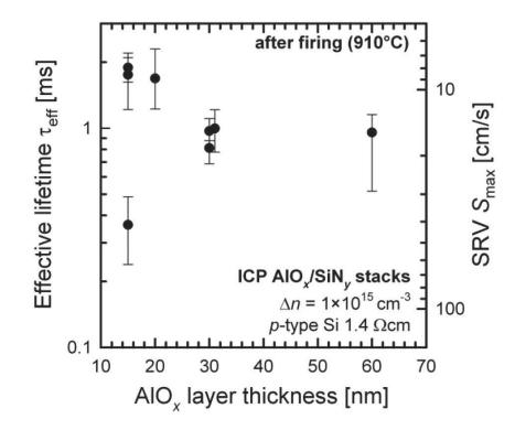
In recent years, Singulus Technologies commercialized the ICP-PECVD process for the deposition of SiNx antireflection layers of silicon solar cells using their SINGULAR tool platform. In this report, we investigate the application of the ICP-PECVD process for the deposition of AlOx layers. We deposit the ICP AlOx layers using a laboratory-type tool at Singulus and investigate the surface passivation properties. We apply ICP AlOx/SiNy layer stacks as rear passivation to large-area PERC solar cells processed at Singulus as well as PERC cells processed at the Q-Cells Research Line.