Gallium nitride is typically grown on sapphire substrates, but this technology is expensive at large diameters. This problem could be solved by growing GaN on silicon wafers. Growth on silicon is complicated because of large difference in thermal expansion coefficient and lattice mismatch between gallium nitride and silicon, which can lead to bowing and furthermore cracking of wafers.
In this work we studied a new method of improving GaN growth on silicon by inserting rare-earth-oxide buffer layers (Er2O3 and Gd2O3) into the structure. We investigated thermal stability of these oxide-coated substrates and crystalline quality of GaN grown on them.
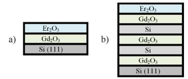
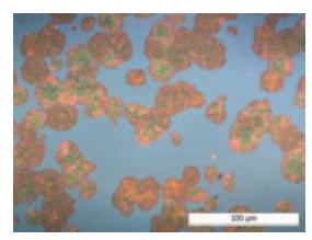
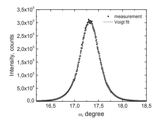
Two types of substrates, provided by Translucent Inc., were investigated – silicon wafer with rare-earth-oxide layers, and distributed Bragg reflectors (DBR) (Fig. 1). Research showed, that silicon wafers with erbium and gadolinium oxide layers (Fig. 1a) were thermally stable at temperatures up to 1050 °C although originally had slightly cracked surface. On these substrates GaN was grown by metalorganic chemical vapor deposition (MOCVD) method. Full width at half maximum (FWHM) of samples GaN (0002) X-ray diffraction (XRD) omega scan was measured to be 822 arcsec. DBR substrate surfaces had no cracks, but were thermally unstable at temperatures higher than 900 °C. Optical microscopy images of those substrates showed damaged regions after annealing (Fig. 3), which might have emerged due to chemical reactions between Si layers and oxides at high temperatures. In both cases the grown GaN layers had a smooth mirror like surface with dense network of cracks.
Because of their thermal stability silicon wafers with rare-earth-oxide layers are suited for GaN growth by MOCVD, but further research is needed in order to produce crack free GaN.